
Multilayer encapsulating process and encapsulating structure of light-emitting diode (LED) driver

A LED driver, multi-layer technology, applied in the field of LED driver multi-layer potting process and potting structure, can solve the problems of large shrinkage rate, lossy power supply, shortened service life, etc., and achieve high power supply stability and heat dissipation High coefficient, the effect of avoiding strain

Inactive Publication Date: 2012-07-18
殷晨钟
View PDF4 Cites 2 Cited by
  • Summary
  • Abstract
  • Description
  • Claims
  • Application Information

AI Technical Summary

Problems solved by technology

[0002] At present, the potting of most LED driving power supplies is single potting with epoxy resin. The thermal conductivity of epoxy resin is not very ideal. shortened service life
In addition, because the epoxy resin is very hard after curing, and has a relatively large shrinkage rate, after potting and curing, some components are easy to be strained, and it is very difficult to repair the cured resin, resulting in product scrapping

Method used


Image

  • Multilayer encapsulating process and encapsulating structure of light-emitting diode (LED) driver
  • Multilayer encapsulating process and encapsulating structure of light-emitting diode (LED) driver
  • Multilayer encapsulating process and encapsulating structure of light-emitting diode (LED) driver

Examples


Embodiment Construction

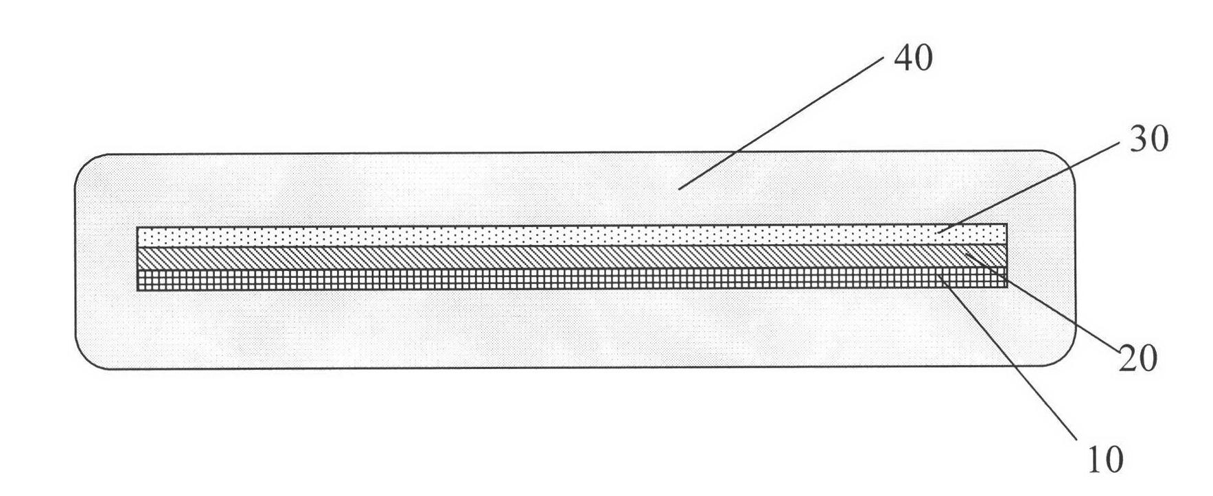
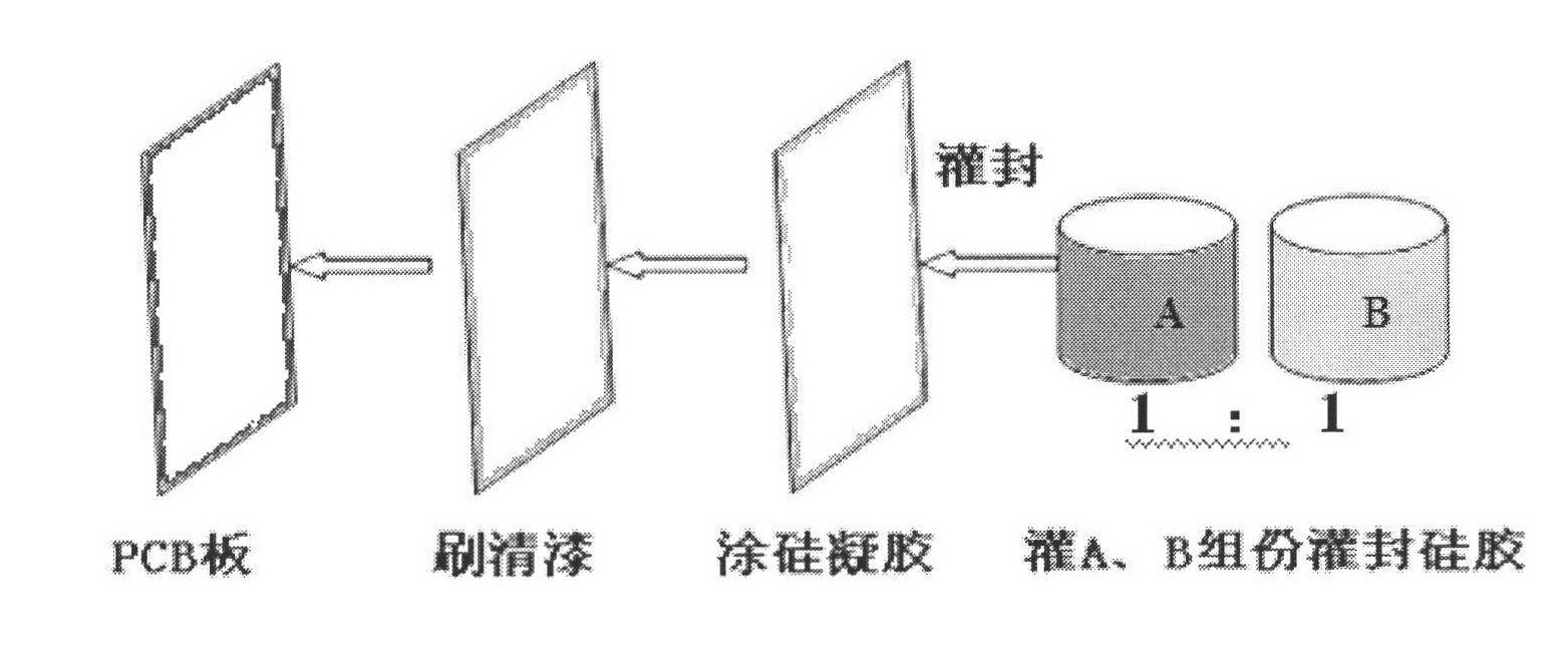
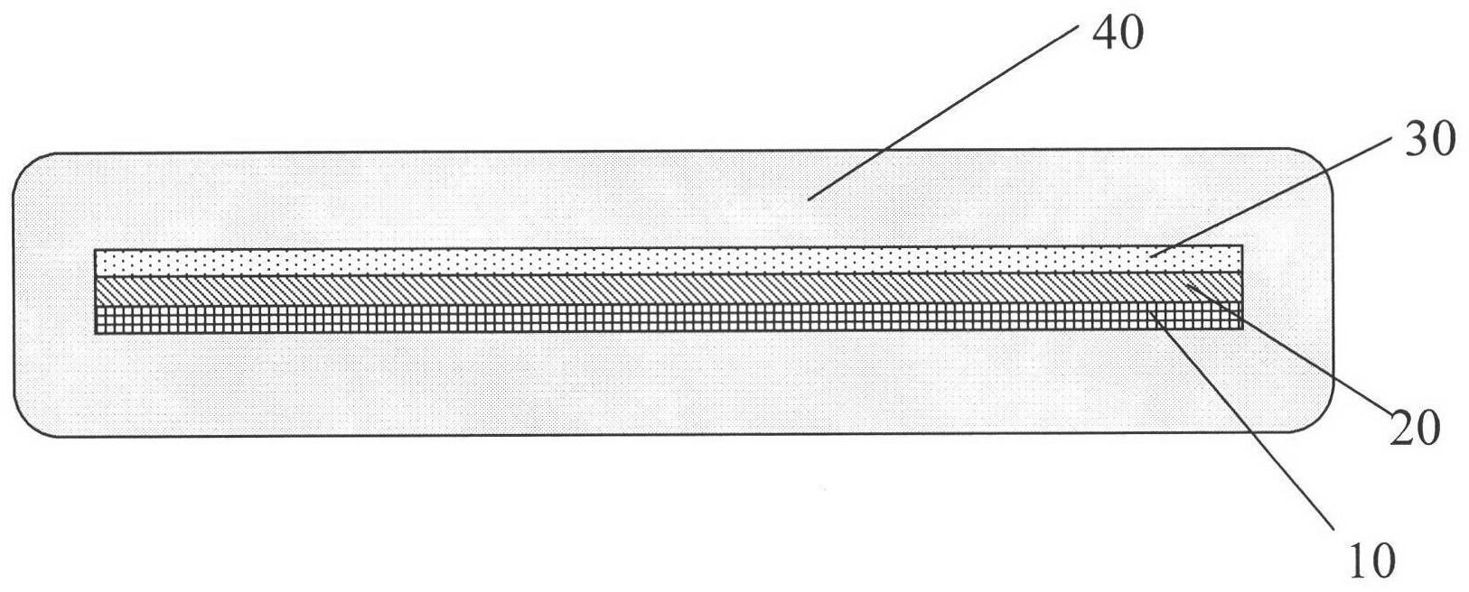
[0009] refer to figure 1 and figure 2 The schematic diagram of the LED driver multi-layer potting structure and potting process flow diagram shown in the present invention, the multi-layer potting process is to first brush a layer of varnish 20 on the patch panel of the finished driver PCB10, and fix it with varnish 20 Components, and then coated with a layer of silicone gel 30, silicone gel can maintain elasticity in the temperature range of -65 ~ 200 ° C for a long time, has excellent electrical properties and chemical stability, water resistance, weather aging resistance, moisture-proof and non-corrosion, insulation , effectively improving the reliability of the power supply; finally, it is perfused with potting silica gel 40, and the potting silica gel is cured to form an elastic solid, which can be shockproof. Since it is an elastic solid, there are no cracks. After curing, due to the softness of the silica gel, it is easy to dig and repair; in addition, the silica gel...


PUM


Abstract

The invention relates to a multilayer encapsulating process and an encapsulating structure of a LED driver, wherein the encapsulating process includes the steps of coating a chip mounting surface of a printed circuit board (PCB) of the driver with a layer of varnish, then coating the surface with a layer of silicon gel, and finally performing integral encapsulation with encapsulating silica gel. The multilayer encapsulating process and the encapsulating structure of the LED driver has the advantages of being water-proof, aging-resistant and corrosion-free, being capable of effectively preventing mounted elements from falling off and being damaged by pulling, being high in radiating coefficient and power supply reliability, and having a shock-proof function due to the elasticity and softness of the solidified encapsulating silica gel.

Description

technical field [0001] The invention relates to the technical field of potting and sealing of electronic components, in particular to a multi-layer potting and sealing process and a potting structure of an LED driver. Background technique [0002] At present, the potting of most LED driving power supplies is single potting with epoxy resin. The thermal conductivity of epoxy resin is not very ideal. Shortened service life. In addition, because the epoxy resin is very hard after curing and has a relatively large shrinkage rate, after potting and curing, some components are easy to be strained, and it is very difficult to repair the cured resin, resulting in product scrapping. Therefore, it is necessary to redesign a potting process and potting structure to solve the above problems. Contents of the invention [0003] In order to solve the problems of heat dissipation of power supply and original device protection caused by single potting of epoxy resin of LED driver in the ...

Claims


Application Information

Patent Timeline
IPC IPC(8): H01L21/56H01L23/29H01L23/31H01L23/373
Inventor 殷晨钟
Owner 殷晨钟
Learn More