Semiconductor device which employs an interlayer insulating film of a low mechanical strength and a highly reliable metal pad, and a method of manufacturing the same

a technology of metal pads and interlayer insulating films, which is applied in the direction of semiconductor devices, semiconductor/solid-state device details, electrical apparatus, etc., can solve the problems of junction failure and cracks, and achieve the effects of reducing the size of the metal pad, reducing the impact stress applied during wire boding, and suppressing a large strain

Inactive Publication Date: 2007-04-10
RENESAS ELECTRONICS CORP +1
View PDF15 Cites 20 Cited by
  • Summary
  • Abstract
  • Description
  • Claims
  • Application Information

AI Technical Summary

Benefits of technology

[0011]However, an impact stress applied during wire boding increases with reduction in size of the metal pad. Therefore, it has been required to provide a lower structure of a metal pad, which can suppress a large strain, and thereby can prevent cracking and peeling of a film.
[0012]An object of the invention is to provide a semiconductor device and a method of manufacturing the same, which can prevent problems, i.e., cracking of an interlayer insulating film and a junction failure due to use of an interlayer insulating film of a low mechanical strength and a low dielectric constant.
[0014]According to the above structure, the interlayer insulating film of the not-low elastic modulus and the metal interconnection layer are located under the metal pad, and the interlayer insulating film of the low elastic modulus is not located under the metal pad. Therefore, the interlayer insulating film of the low elastic modulus, in which a crack may occur in a wire bond, does not directly receive an impact stress caused by the wire bonding so that the crack can be prevented. It is also possible to suppress a strain, which may occur at an interface between the metal interconnection layer and the interlayer insulating film of the not-low elastic modulus, so that it is possible to prevent reliably the interlayer insulating film of the low elastic modulus from peeling at a position shifted from a position immediately under the metal pad.
[0016]The above method can easily form a metal pad structure of high reliability.

Problems solved by technology

Due to the lowering of mechanical strength of the interlayer insulating film, a crack may occur in the interlayer insulating film arranged in the layer under the metal pad, or a junction failure may occur in wire-bond when probing is executed for wire bonding or device test.

Method used


Image

  • Semiconductor device which employs an interlayer insulating film of a low mechanical strength and a highly reliable metal pad, and a method of manufacturing the same
  • Semiconductor device which employs an interlayer insulating film of a low mechanical strength and a highly reliable metal pad, and a method of manufacturing the same
  • Semiconductor device which employs an interlayer insulating film of a low mechanical strength and a highly reliable metal pad, and a method of manufacturing the same

Examples


second embodiment

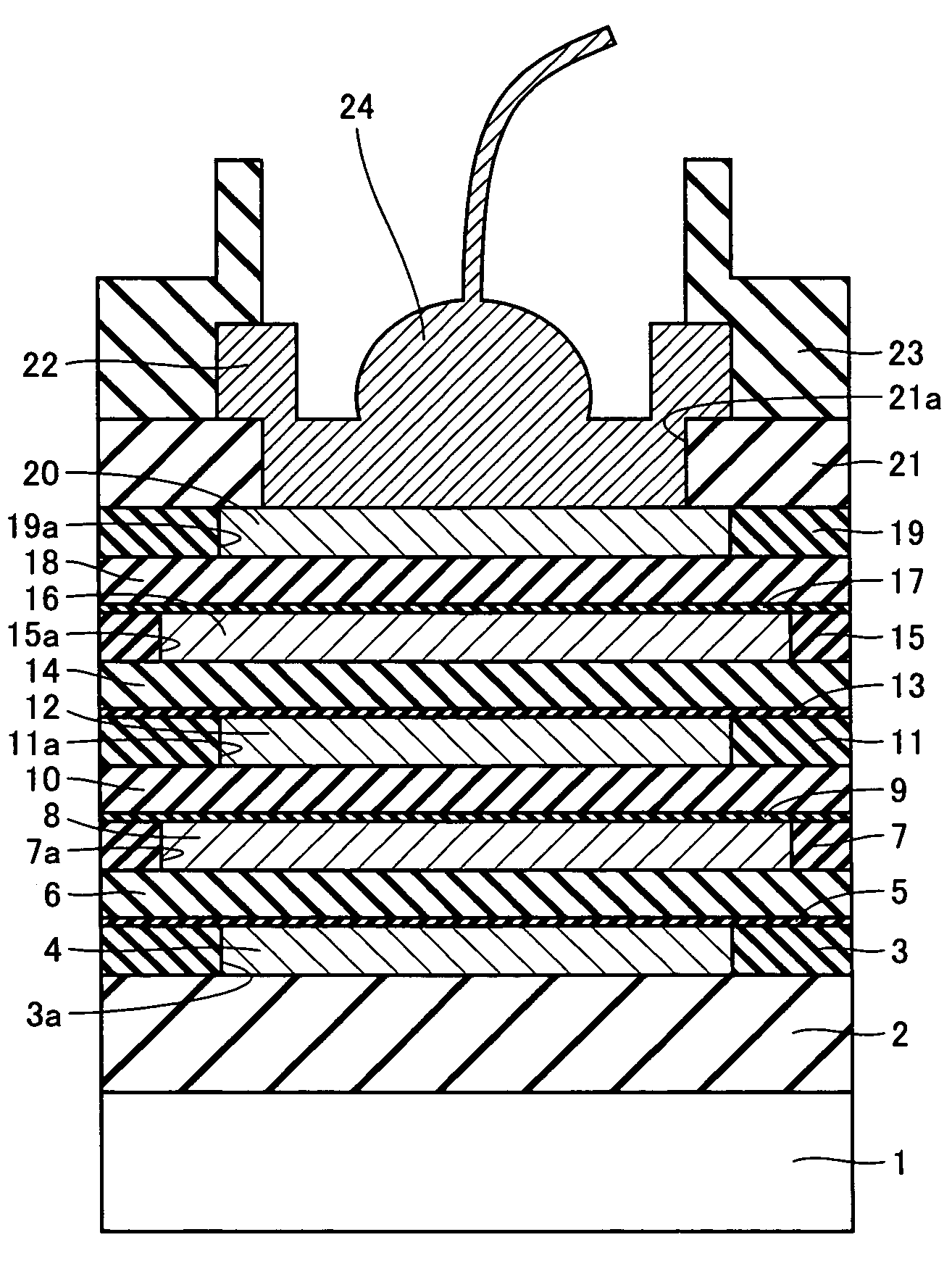
[0039](Second Embodiment)

[0040]FIG. 3 shows a structure of a metal pad of a semiconductor device according to a second embodiment of the invention. A method of forming the interlayer insulating films and the copper interconnections is completely the same as that in the first embodiment, and therefore description thereof is not repeated.

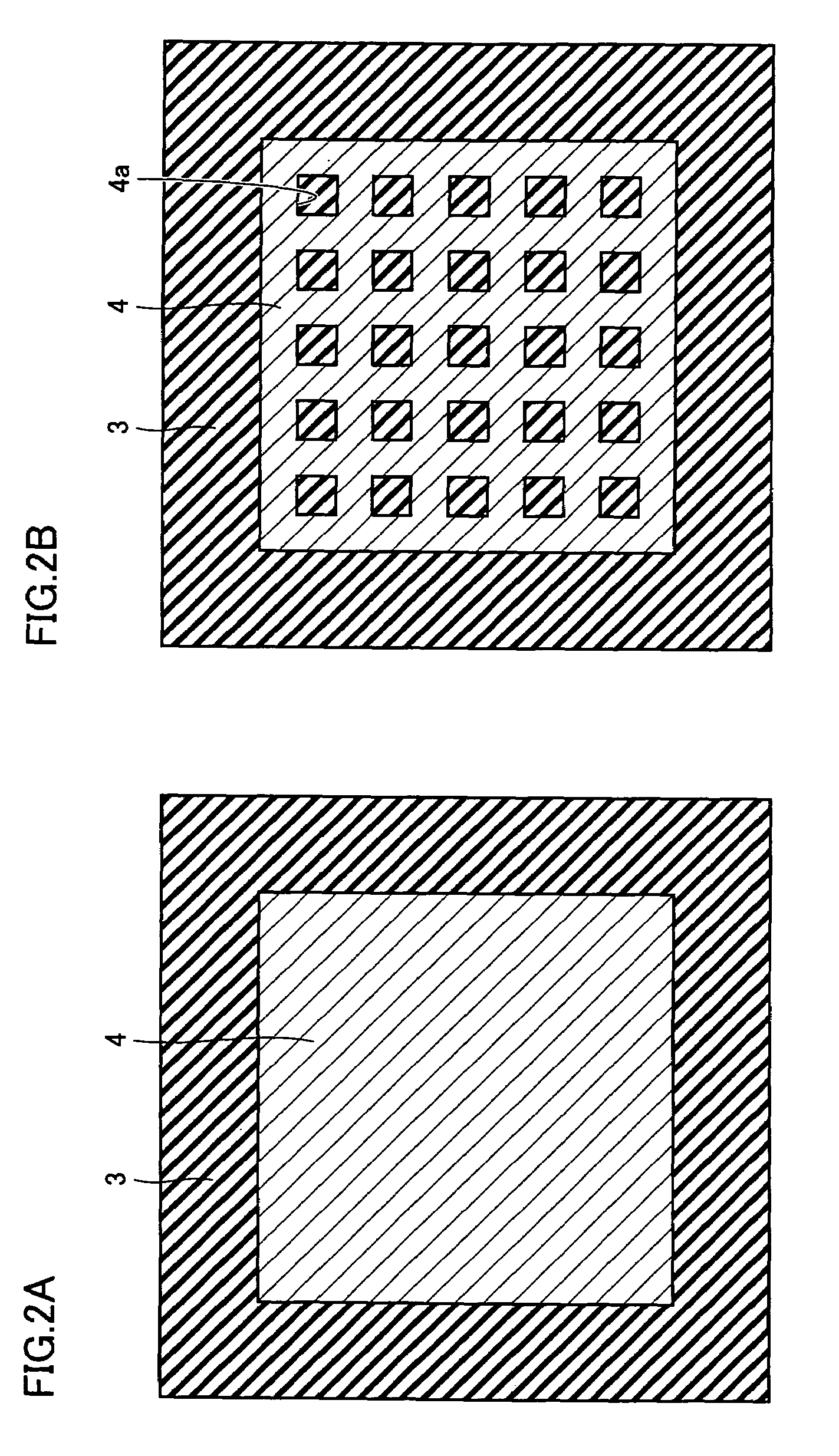
[0041]The second embodiment of the invention differs from the first embodiment in that the copper interconnection in each layer fills the connection aperture under it. More specifically, second copper interconnection 8 in the second layer fills connection apertures 5a and 6a. In the third layer, a third copper interconnection 12 fills connection apertures 9a and 10a. Likewise, a fourth layer includes a fourth copper interconnection 16 filling connection apertures 13a and 14a, and a fifth layer includes fifth copper interconnection 20 filling connection apertures 17a and 18a. The connection apertures described above may be merely referred to as “apertu...

third embodiment

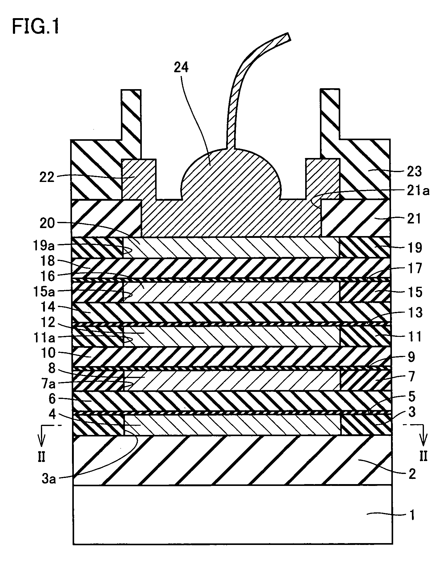
[0044](Third Embodiment)

[0045]FIG. 5 shows a structure of a metal pad of a semiconductor device according to a third embodiment of the invention. A method of forming the interlayer insulating films and the copper interconnections in this embodiment is completely the same as that in the first embodiment, and therefore description thereof is not repeated. The third embodiment differs from the first embodiment in that copper interconnections 4, 8, 12, 16 and 20 arranged in openings 3a, 7a, 11a, 15a and 19a, which are provided at the interlayer insulating films of low elastic moduli in the respective layers, do not have uniform planar sizes. More specifically, the copper interconnection in each layer has a planar size different from that of the copper interconnection(s) in a vertically neighboring layer(s). Copper interconnection 8 in the second layer has a larger planar size than copper interconnection 4 in the first layer. The copper interconnections in the third and fifth layers have...


PUM


Abstract

A semiconductor device includes: multiple kinds of interlayer insulating films formed on a semiconductor substrate and having different elastic moduli, respectively; a metal pad arranged on said multiple kinds of interlayer insulating films; the interlayer insulating film of a low elastic modulus having the lowest elastic modulus and having an opening located under the metal pad, the interlayer insulating film of a not-low elastic modulus having the elastic modulus larger than the elastic modulus of the interlayer insulating film of the low elastic modulus, being layered in contact with the interlayer insulating film of the low elastic modulus, and continuously extending over the opening and a region surrounding the opening and a metal interconnection layer arranged under the metal pad, filling the opening in the interlayer insulating film of the low elastic modulus, and being in contact with the interlayer insulating film of the not-low elastic modulus.

Description

BACKGROUND OF THE INVENTION[0001]1. Field of the Invention[0002]The present invention relates to a semiconductor device and a method of manufacturing the same, and particularly relates to a semiconductor device, which employs an interlayer insulating film of a low mechanical strength and a low dielectric constant, and has a highly reliable metal pad, as well as a method of manufacturing the same.[0003]2. Description of the Background Art[0004]In system LSIs in and after 0.18-micron generation, it is important to reduce signal delays in devices for achieving fast operations. The signal delay in the device is represented by a sum of a signal delay in a transistor and an interconnection delay, and the influence by the interconnection delay has been increasing with rapid reduction in interconnection pitch, as compared with the signal delay in the transistor. Since the interconnection delay is proportional to a product (R×C) of a resistance (R) and an interlayer capacitance (C), lowering...

Claims


Application Information

Patent Timeline
Patent Type & Authority Patents(United States)
IPC IPC(8): H01L23/48H01L23/52H01L29/40H01L21/3205H01L21/60H01L21/768H01L23/485H01L23/532
CPCH01L23/5329H01L24/03H01L24/05H01L24/48H01L2224/02166H01L2224/04042H01L2224/05009H01L2224/05073H01L2224/05093H01L2224/05096H01L2224/05181H01L2224/05187H01L2224/05554H01L2224/05624H01L2224/48091H01L2224/48463H01L2224/85424H01L2224/85447H01L2924/01004H01L2924/01005H01L2924/01006H01L2924/01007H01L2924/01013H01L2924/01014H01L2924/01029H01L2924/01033H01L2924/01073H01L2924/01078H01L2924/01079H01L2924/01082H01L2924/04953H01L2924/05042H01L2924/14H01L2924/19043H01L2924/30105H01L2924/00014H01L2924/04941H01L2924/01019H01L2224/45099H01L2224/05558H01L21/3205H01L21/768H01L21/60
Inventor MATSUURA, MASAZUMIHORIBE, HIROSHIMATSUMOTO, SUSUMUHAMATANI, TSUYOSHI
Owner RENESAS ELECTRONICS CORP
Why Eureka
Try Eureka