High-power high-brightness light-emitting diode (LED) light source packaging structure and packaging method thereof

A technology of LED light source and packaging method, applied in the field of LED light source, can solve the problems of poor stability, thermal expansion coefficient mismatch between LED chip and heat sink, low heat dissipation efficiency of LED packaging structure, etc., achieve stable performance, simple structure, and enhanced heat dissipation capacity Effect

Active Publication Date: 2012-07-18
FOCUSLIGHT TECH
View PDF5 Cites 6 Cited by
  • Summary
  • Abstract
  • Description
  • Claims
  • Application Information

AI Technical Summary

Problems solved by technology

[0013] The purpose of the present invention is to overcome the shortcomings of the above-mentioned prior art, and provide a high-power and high-brightness LED light source packaging method and packaging structure. The present invention can solve the problem of heat dissipation of the LED packaging structure in the prior art by optimizing the design of the LED light source packaging structure. The problem of low efficiency and poor stability can be improved, and the problem of thermal expansion coefficient mismatch between the LED chip and the heat sink can be improved

Method used


Image

  • High-power high-brightness light-emitting diode (LED) light source packaging structure and packaging method thereof
  • High-power high-brightness light-emitting diode (LED) light source packaging structure and packaging method thereof
  • High-power high-brightness light-emitting diode (LED) light source packaging structure and packaging method thereof

Examples


Embodiment Construction

[0053] The present invention is described in further detail below in conjunction with accompanying drawing:

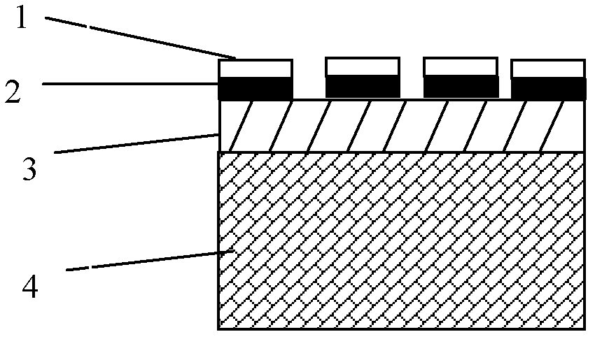
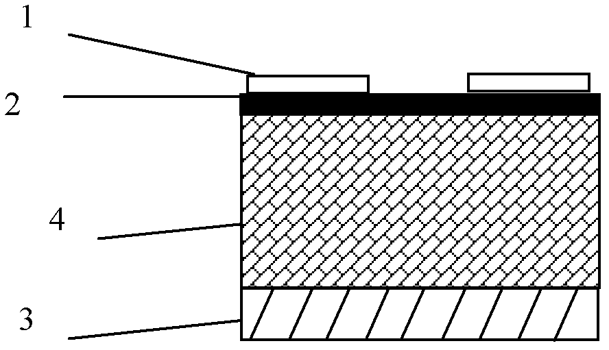
[0054] figure 1 It is the structural diagram of the first LED module of the present invention. A stress relief layer is set on the bottom surface of the LED chip (non-luminous surface) to reduce the thermal stress of the LED chip. figure 1 For the material of the stress-releasing layer in contact with the bottom surface (non-luminous surface) of the 4 LED chips, the difference between the thermal expansion coefficient and the LED chip is less than 40%, and 0.05mm thick aluminum nitride ceramics can be selected as the stress-releasing layer. Solder, such as gold-tin solder, is welded with the LED chip, and then an insulating layer is provided. The material of the insulating layer can be ceramic or diamond, and then the heat dissipation base is used to conduct contact heat dissipation treatment on the chip. The material of the heat dissipation base can be selected with h...


PUM


Abstract

The invention discloses a high-power high-brightness light-emitting diode (LED) light source packaging structure and a packaging method thereof. The packaging structure provided by the invention comprises a radiation board, a circuit board and an LED module, wherein the LED module is manufactured by performing contact-type radiation treatment, thermal stress reduction treatment and insulation treatment on an LED chip; the LED module is welded on the radiation board; and the circuit board is welded or adhered to the radiation board, so that the circuit board is distributed on the periphery of the LED module and is electrically connected with the LED chip. According to the invention, through the optimal design of the LED light source packaging structure, the problems of low radiation efficiency and poor stability of the LED packaging structure in the prior art can be solved, the problem that the LED chip is mismatched with a heat sink thermal expansion coefficient is solved, and the packaging structure has the advantages of high stability, long storage life, low cost and the like.

Description

technical field [0001] The invention belongs to the technical field of LED light sources and relates to packaging of LED light sources, in particular to a high-power and high-brightness LED light source packaging structure and a packaging method thereof. Background technique [0002] Light sources commonly used in projection display systems are ultra-high pressure mercury lamps (UHP), metal halide lamps, xenon lamps, and halogen lamps. Human beings have been looking for and developing solid-state light sources for many years. With the development of light-emitting materials and the improvement of semiconductor manufacturing processes, the efficiency of light-emitting diodes for semiconductor lighting has continued to increase. At present, the ultra-high pressure mercury lamp is the mainstream light source of the projection device. Light-emitting diodes (LEDs for short) are a type of semiconductor device that directly converts electrical energy into light energy. LED has a ...

Claims


Application Information

Patent Timeline
Patent Type & Authority Applications(China)
IPC IPC(8): H01L33/48H01L33/64F21V29/00F21Y101/02F21V29/503F21V29/70F21V29/85F21Y115/10
Inventor 刘兴胜李小宁宗恒军郑艳芳王警卫
Owner FOCUSLIGHT TECH
Why Eureka
Try Eureka