Level transfer circuit

A technology for transferring circuits and levels, which is applied in the direction of logic circuit connection/interface layout, logic circuit coupling/interface using field effect transistors, etc. It can solve the problems of reducing circuit conversion speed and increasing transient current, achieving fast speed, Effect of Improving Circuit Speed

Inactive Publication Date: 2012-07-18
SUZHOU PIXCIR MICROELECTRONICS
View PDF3 Cites 2 Cited by
  • Summary
  • Abstract
  • Description
  • Claims
  • Application Information

AI Technical Summary

Problems solved by technology

[0004] When the level of the input pin IN changes from low level to high level, the P-type transistor P1 and N-type transistor N1 and the P-type transistor P2 and N-type Transistor N2 will be turned on at the same time during a transient period, and a through current will be generated between the high potential of the power supply VDD and the low potential of the source power supply VSS, increasing the transient current and reducing the switching speed of the circuit at the same time

Method used


Image

  • Level transfer circuit
  • Level transfer circuit
  • Level transfer circuit

Examples


Embodiment Construction

[0010] The present invention will be further described below in conjunction with the accompanying drawings and embodiments.

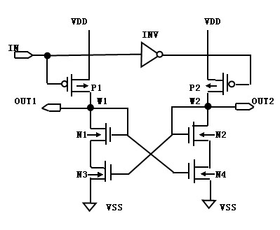
[0011] Please refer to figure 1 The first type of level shifting circuit shown includes a P-type transistor P1 and a P-type transistor P2, the source of the P-type transistor P1 and the source of the P-type transistor P2 are respectively connected to the power supply VDD, and the gate of the P-type transistor P1 is connected to Input pin IN, an inverter INV is provided between the gates of the P-type transistor P1 and P-type transistor P2; the drain of the P-type transistor P1 is the output channel OUT1, and the drain of the P-type transistor P1 is connected to the N-type transistor N1 The gate of the drain and N1, and the gate of the N-type transistor N1 is connected to the gate of the N-type transistor N4, the source of the N-type transistor N1 is connected to the drain of the N-type transistor N3, and the source of the N-type transistor N3 Conn...


PUM


Abstract

The invention relates to a level transfer circuit. The level transfer circuit comprise a P type transistor P1 and a P type transistor P2, wherein an inverter INV is arranged between grid electrodes of the P type transistor P1 and the P type transistor P2, a drain electrode of the P type transistor P1 is connected with a drain electrode of an N type transistor N1 and a grid electrode of the N type transistor N1, the grid electrode of the N type transistor N1 is connected with a grid electrode of an N type transistor N4, a drain electrode of the P type transistor P2 is connected with a drain electrode of an N type transistor N2 and a grid electrode of the N type transistor N2, and the grid electrode of the N type transistor N2 is connected with a grid electrode of an N type transistor N 3. The level transfer circuit of the invention not only can adopt a miniature device, but also is not related to the process change, and the circuit speed can be improved; furthermore, a symmetrical structure layout is adopted, so that the layout is quick and easy; and designers can draw alternatively without the technology change.

Description

technical field [0001] The invention relates to a circuit, in particular to a level transfer circuit which can use small devices and has nothing to do with process changes. Background technique [0002] A level shift circuit is a circuit that performs signal amplitude conversion on circuits of different levels, and is often used for communication between control signals output by low power supply voltage circuits and high power supply voltage circuits. [0003] The level shifting circuit commonly used at present is very easy to generate a through current during the change of the input signal level. In the case of multiple level shifting circuits with the same structure, it will lead to an increase in power consumption of the circuit. like figure 1 Shown is a circuit diagram of an existing level shifting circuit, and its structure is as follows: the potential of the power supply VDD is at a high level, and the potential of the source power supply VSS is at a low level, and t...

Claims


Application Information

Patent Timeline
Patent Type & Authority Applications(China)
IPC IPC(8): H03K19/0185
Inventor 保罗·格兰德维兹
Owner SUZHOU PIXCIR MICROELECTRONICS
Why Eureka
Try Eureka