

Liquid crystal display device and driving method therefor
A technology of a liquid crystal display device and a driving method, which can be applied to static indicators, instruments, etc., and can solve the problems of display quality degradation and the like
- Summary
- Abstract
- Description
- Claims
- Application Information
AI Technical Summary
Problems solved by technology
Method used
Image

Examples
no. 1 approach
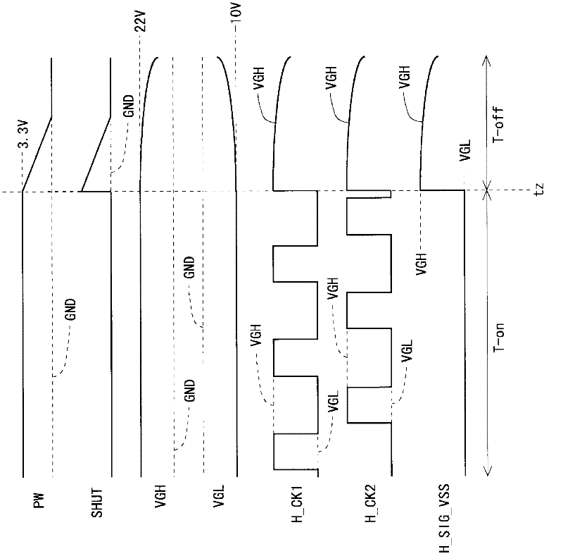
[0100]
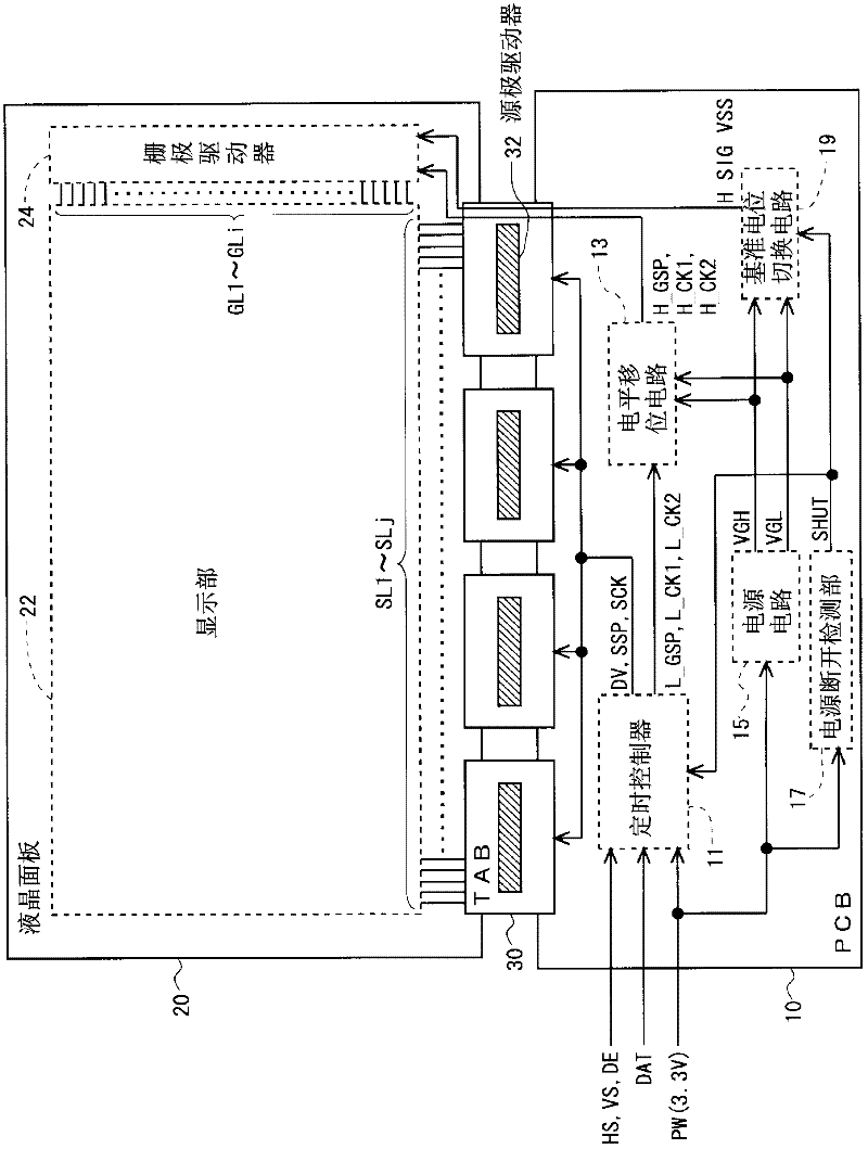
[0101] figure 2 It is a block diagram showing the overall configuration of the active matrix liquid crystal display device according to the first embodiment of the present invention. Such as figure 2 As shown, the liquid crystal display device includes a liquid crystal panel 20 , a PCB (printed circuit board) 10 and a TAB (Tape Automated Bonding) 30 connecting the liquid crystal panel 20 and the PCB 10 .
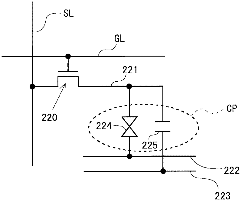
[0102] On the liquid crystal panel 20, a display portion 22 for displaying an image is formed. The display section 22 includes: multiple (j) source bus lines (video signal lines) SL1˜SLj; multiple (i) gate bus lines (scanning signal lines) GL1˜GLi; A plurality of (i×j) pixel forming portions provided corresponding to intersections of ˜SLj and gate bus lines GL1 ˜GLi. image 3 It is a circuit diagram showing the structure of a pixel formation part. Such as image 3 As shown, each pixel forming part includes: a thin film transistor (TFT) 220, the gate termina...
PUM
 Abstract
Description
Claims
Application Information