Multi-beam parallel laser direct writing device and method

A laser direct writing and multi-beam technology, which is applied in photolithographic exposure devices, microlithography exposure equipment, optics, etc., can solve the problem of unstable laser light source energy during processing, and achieve the effect of improving processing efficiency

Inactive Publication Date: 2012-08-01
SHANGHAI INST OF OPTICS & FINE MECHANICS CHINESE ACAD OF SCI
View PDF5 Cites 36 Cited by
  • Summary
  • Abstract
  • Description
  • Claims
  • Application Information

AI Technical Summary

Problems solved by technology

Theoretically, the laser direct writing technology using the two-photon absorption effect can produce a feature size smaller than the Ray...

Method used


Image

  • Multi-beam parallel laser direct writing device and method
  • Multi-beam parallel laser direct writing device and method
  • Multi-beam parallel laser direct writing device and method

Examples


Embodiment Construction

[0032] The present invention will be further described below in conjunction with the specific application of the manufacturing process and the accompanying drawings, but the application of the present invention is not limited thereto.

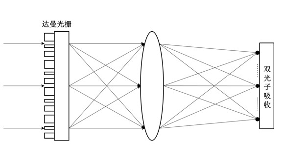
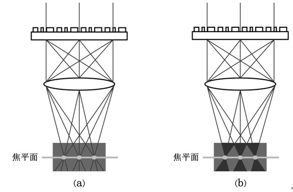
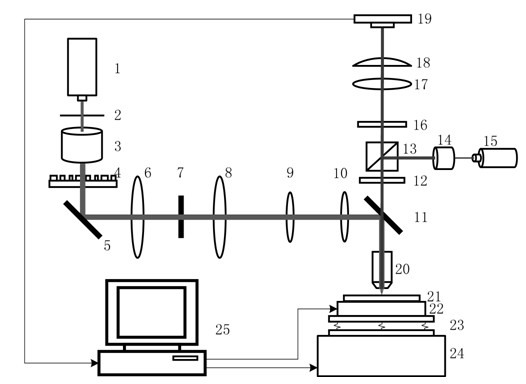
[0033] see first image 3 , image 3It is the optical path structure diagram of the multi-beam parallel laser direct writing device of the present invention. It can be seen from the figure that the multi-beam parallel laser direct writing device of the present invention includes a writing optical path, a detection optical path, a three-dimensional moving mechanism and a computer, and its characteristics are:

[0034] The writing optical path includes a femtosecond laser 1, and along the laser output advancing direction of the femtosecond laser 1, there are successively an aperture stop 2, a beam expander lens group 3, a Damman grating 4, a first beam expander lens 6, a gradient Refractive index filter 7, second beam expander lens 8, transfer ...


PUM


Abstract

The invention discloses a multi-beam parallel laser direct writing device and a multi-beam parallel laser direct writing method. A Dammann grating beam-splitting device is combined with two-photon absorption, so that the device has the characteristics of high stability and high resolution ratio, a periodic micro-nano structure is easily manufactured, and the processing efficiency can be improved by hundreds of times. The multi-beam parallel laser direct writing device and the multi-beam parallel laser direct writing method are suitable for processing and industrial production of large-area periodic micro-nano optical structures.

Description

technical field [0001] The invention relates to optical micro-nano structure processing, in particular to a multi-beam parallel laser direct writing device and a direct writing method thereof. Background technique [0002] In the past few decades, great progress has been made in the field of optics and photonics. For example, the progress of optical waveguide structure, photoelectric energy conversion, solid-state lighting device, laser and optical sensor has benefited from the development of two-dimensional lithography technology. Microelectronics processing technology is rapidly developing toward the nanometer scale, and photolithography technology in the optical field has also developed rapidly in recent years. Three-dimensional photonic circuit technology based on three-dimensional complete photonic bandgap structure has also become mature in recent years. For the processing of "chiral" photonic crystal functional materials in the three-dimensional photonic crystal stru...

Claims


Application Information

Patent Timeline
IPC IPC(8): G03F7/20G02B27/28G02B5/18
Inventor 朱锋周常河麻健勇
Owner SHANGHAI INST OF OPTICS & FINE MECHANICS CHINESE ACAD OF SCI
Why Eureka
Try Eureka