Display device, array substrate and manufacturing method thereof

A technology of an array substrate and a manufacturing method, applied in the field of display devices, can solve the problems of low production efficiency, complex array substrate fabrication, increase of liquid crystal panels, etc., and achieve the effects of saving production costs, reducing production costs, and reducing etching

Active Publication Date: 2012-08-08
BOE TECH GRP CO LTD
View PDF3 Cites 10 Cited by
  • Summary
  • Abstract
  • Description
  • Claims
  • Application Information

AI Technical Summary

Problems solved by technology

[0007] The technical problem to be solved by the present invention is to provide a display device, an array substrate and a manufacturing method thereof, so as to overcome the need to add an additional barrier layer to protect the metal oxide (such as IGZO) active layer from being damaged in the existing array substrate. The production of the array substrate caused by layers is complicated, the production efficiency is low, and the production cost of display devices such as liquid crystal panels is increased.

Method used


Image

  • Display device, array substrate and manufacturing method thereof
  • Display device, array substrate and manufacturing method thereof
  • Display device, array substrate and manufacturing method thereof

Examples


Embodiment approach

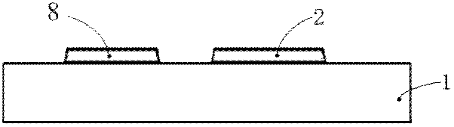
[0054] A specific implementation is as follows: reference Figure 2e , on the substrate after step S3, a gate metal thin film is deposited, and a gate electrode 6 is formed by using a common mask plate through masking, exposure, etching and photoresist removal processes, and the thickness of the gate electrode 6 is 2200 angstroms.

[0055] In order to better protect the devices on the array substrate, this embodiment may further include the following steps:

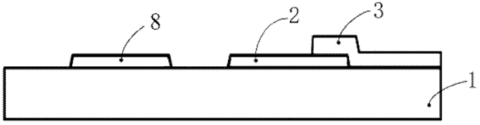
[0056] That is, step S5, forming a protective layer on the substrate after step S4 by adopting the fifth patterning process.

[0057] Specifically: reference Figure 2f , on the substrate after step S4, deposit a protective layer thin film, and use a common mask to form the protective layer 7 through masking, exposure, etching and photoresist removal processes.

[0058] In the embodiment of the present invention, the specific implementation of each step, especially the description about the method of forming the film la...


PUM


Abstract

The invention relates to the technical field of display, in particular to a display device, an array substrate and a manufacturing method thereof. The array substrate comprises a substrate and a plurality of pixel units; each pixel unit comprises a thin film transistor and a pixel electrode; the thin film transistor comprises a source electrode, a drain electrode, an active layer, a grid electrode insulating layer and a grid electrode, wherein the source electrode and the drain electrode are oppositely arranged on the substrate and forms a channel of the thin film transistor; the active layer is positioned above the source / drain electrode and the channel; the grid electrode insulating layer and the grid electrode are arranged above the active layer in sequence; and the pixel electrode is positioned in an area outside the thin film transistor in the pixel unit and extends to the upper part of the drain electrode and is overlapped with the drain electrode. Through the array substrate provided by the invention, as the active layer is positioned above the source / drain electrode, the active layer can be prevented from being damaged in the forming process of the source / drain electrode. Moreover, when the active layer is made of metallic oxide, a blocking layer can be omitted, and further, the process flow is simplified, the production efficiency is improved, and the production cost is reduced.

Description

technical field [0001] The present invention relates to the field of display technology, in particular to a display device, an array substrate and a manufacturing method thereof. Background technique [0002] In recent years, with the development of science and technology, liquid crystal display technology has also been continuously improved. TFT-LCD (Thin Film Transistor-Liquid Crystal Display, Thin Film Field Effect Transistor-Liquid Crystal Display) occupies an important position in the display field due to its advantages of good image display quality, low energy consumption, and environmental protection. [0003] While people are enjoying the high-quality image display of liquid crystal displays, their requirements for large sizes are also constantly increasing. When the size of the liquid crystal display increases continuously, the frequency of its driving circuit also needs to be continuously increased, and accordingly the mobility of the amorphous silicon transistor ...

Claims


Application Information

Patent Timeline
Patent Type & Authority Applications(China)
IPC IPC(8): H01L27/12H01L21/77G02F1/1362G02F1/1368
CPCG02F1/1368H01L21/77H01L27/1225G02F1/1362H01L27/12H01L27/124G02F1/13685
Inventor 童晓阳曹占锋
Owner BOE TECH GRP CO LTD
Why Eureka
Try Eureka