Spinning microwave oscillator based on vertical magnetizing free layer and manufacturing method thereof

A microwave oscillator, vertical magnetization technology, applied in resonators, waveguide-type devices, electrical components, etc., can solve the problem of low output power of spin microwave devices, and achieve the effects of broadband adjustable integration, low cost, and small size

Active Publication Date: 2012-08-15
SUZHOU INST OF NANO TECH & NANO BIONICS CHINESE ACEDEMY OF SCI
View PDF8 Cites 19 Cited by
  • Summary
  • Abstract
  • Description
  • Claims
  • Application Information

AI Technical Summary

Problems solved by technology

[0004] However, at present, the "bottleneck" problem encountered in the preparation and application of spin microwave oscillators in the world is: in most of the existing technologies, the microwave output can only be realized under the condition of applying an external magnetic field, which gives The manufacture and future practical application of the device brings technical challenges, and the output power of the spin microwave device manufactured by the existing technology is low

Method used


Image

  • Spinning microwave oscillator based on vertical magnetizing free layer and manufacturing method thereof
  • Spinning microwave oscillator based on vertical magnetizing free layer and manufacturing method thereof
  • Spinning microwave oscillator based on vertical magnetizing free layer and manufacturing method thereof

Examples


Embodiment 1

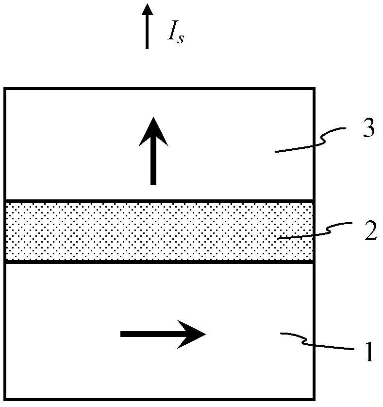
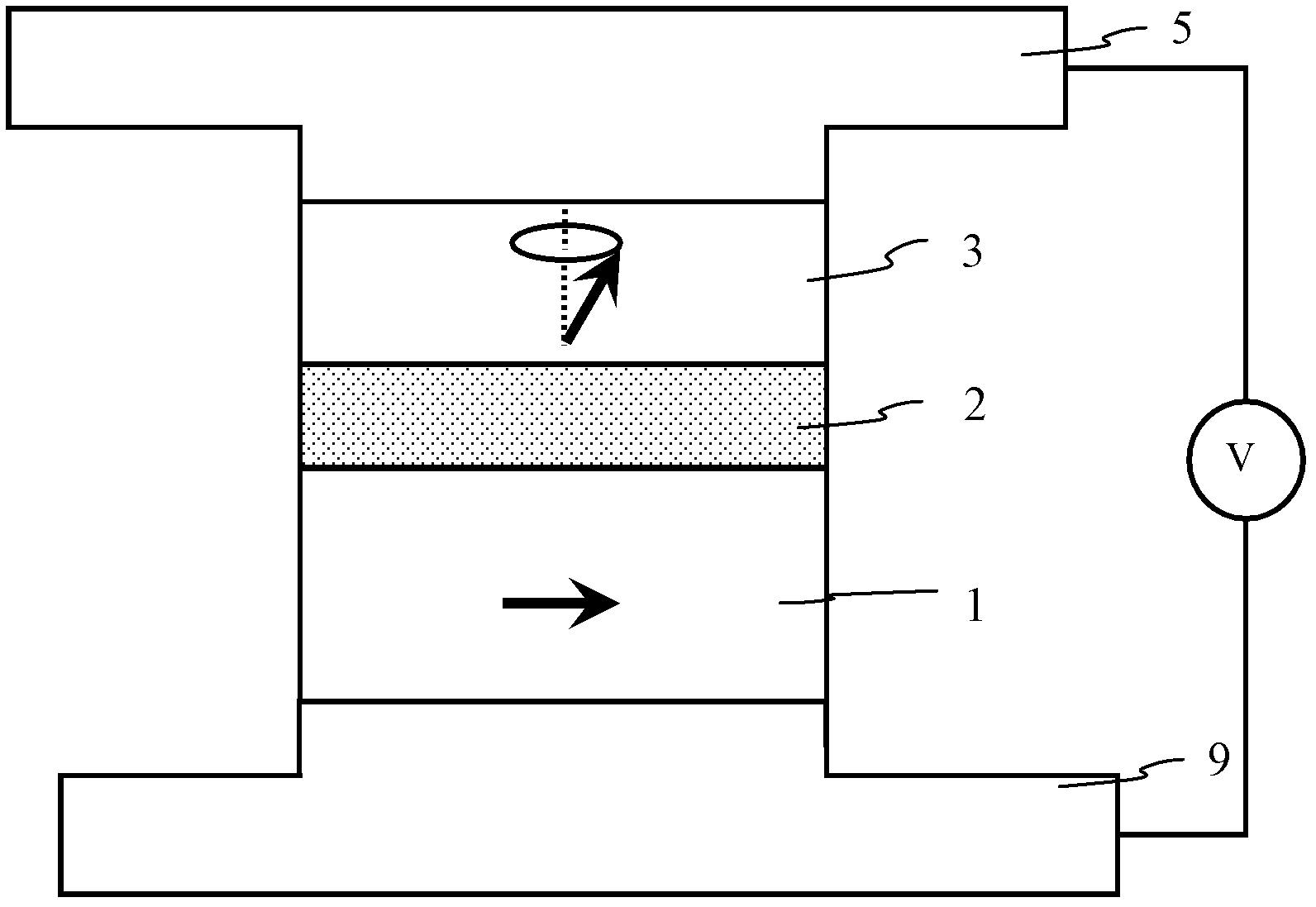
[0041] Example 1 refer to figure 2 , the structure of the spin microwave oscillator based on the perpendicular magnetization free layer and in-plane magnetization fixed layer structure is as follows: firstly a CuN seed layer 9 is formed on the substrate; then a lower ferromagnetic Co 40 Fe 40 B 20 layer, its thickness is 2 nm, and the magnetization direction of the layer is parallel to the surface of the film; one formed on the ferromagnetic Co 40 Fe 40 B 20 A spacer layer above the spacer layer, that is, a MgO barrier layer with a thickness of 0.8 nm; another magnetic Co 20 Fe 60 B 20 layer and a CuN capping layer formed over the second ferromagnetic layer. co 20 Fe 60 B 20 The magnetization direction of the layer is perpendicular to the film plane and forms an angle of about 90 degrees with the first magnetic material layer without a magnetic field, Co 20 Fe 60 B 20 The magnetization direction of the layer changes in response to an applied magnetic field as w...

Embodiment 2

[0043] Example 2 In the foregoing embodiments, the balanced magnetization direction of the first magnetic layer is determined by the in-plane magnetization of the material, and its direction is relatively fixed. But when its coercive force is small, its magnetization direction can be reversed under the action of a small external field, thereby affecting the microwave performance of the microwave oscillator. In view of the above problems, this embodiment further proposes a pinned microwave oscillator, the structure of which is as follows Figure 4 As shown, that is: firstly a seed layer is formed on the substrate; then an antiferromagnetic layer is formed on the seed layer, and the lower ferromagnetic layer or semi-metal layer (reference layer) is formed on the antiferromagnetic layer, and the reference layer’s The equilibrium magnetization direction is relatively fixed due to the pinning effect of antiferromagnetism; a nonmagnetic isolation layer formed on the reference laye...

Embodiment 3

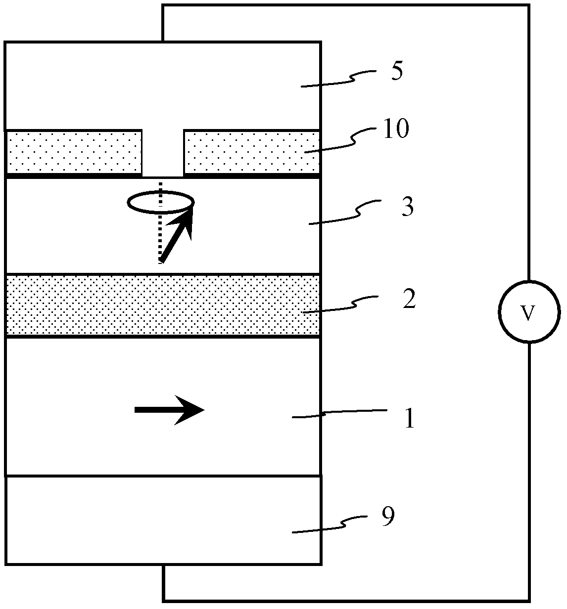
[0045] Example 3 In the foregoing embodiment 2, the antiferromagnetic layer 4 pinning the ferromagnetic or half-metal layer 1 can also be composed of the antiferromagnetic layer 4 and the ferromagnetic layer / nonmagnetic metal layer / ferromagnetic layer (FM / NM / FM) The FM / NM / FM composite multilayer film forms an artificial antiferromagnetic coupling layer, so that the magnetization direction of the magnetic layer 1 is fixed. Here FM is similar to the material of the lower magnetic layer 1 in Example 1, and NM is composed of non-magnetic metals such as Ru, Cu, Ag, etc., and its thickness is about 0.8 nm, which meets the requirements of FM / NM / FM composite multilayer film to form artificial antiferromagnetism The coupling condition, its basic structure is as Figure 5 shown. An example of a specific material is given here, in Si / SiO 2 On the substrate, a seed layer (3 nm Ta / 10 nm CuN / 5 nm Ta), an antiferromagnetic layer 4 (15 nm IrMn), an artificial antiferromagnetic coupling ...


PUM


Abstract

The invention discloses a spinning microwave oscillator based on a vertical magnetizing free layer and a manufacturing method of the spinning microwave oscillator. The spinning microwave oscillator comprises a magnetic multilayer film and electrodes connected with the magnetic multilayer film, wherein the magnetic multilayer film comprises a seed layer, a first magnetic layer, a non-magnetic isolating layer, a magnetic free layer and a protecting layer; the first magnetic layer is formed on the seed layer and has an in-plane balanced magnetizing state; the non-magnetic isolating layer is formed on the first magnetic layer; the magnetic free layer with vertical magnetization is formed on the non-magnetic isolating layer; and the protecting layer is formed on the free layer. The manufacturing method of the spinning microwave oscillator comprises the steps of: forming the magnetic multilayer film on a substrate according to a magnetron sputtering method; processing the magnetic multilayer film into a nanometer columnar or point contact structure according to microelectronic technology; and arranging upper and lower electrodes on the magnetic multilayer film so as to form a target product. The spinning microwave oscillator can obtain high microwave power output without externally added magnetic field; the spinning microwave oscillator has the characteristics of small size, simple structure, adjustable broadband, easiness in integration and the like; the preparation is easily realized; and the cost is low.

Description

technical field [0001] The invention generally relates to the technical field of spin transport devices, in particular to microwave oscillators applied in the field of wireless communication. Background technique [0002] With the rapid development of mobile communications and satellite communications, the requirements for miniaturization and integration of devices are becoming more and more urgent. Take mobile phones as an example. At present, there are hundreds of passive electronic components in each mobile phone. Therefore, the miniaturization and integration of passive electronic components play a decisive role in the portability of mobile phone products. At the same time, mobile communication is also developing towards high frequency and broadband. The frequency band used by the early first-generation mobile communication is between 800 MHz and 900 MHz, and the frequency band used by the second-generation mobile communication, which is mainly characterized by digital s...

Claims


Application Information

Patent Timeline
Patent Type & Authority Applications(China)
IPC IPC(8): H01P7/00H01P11/00
Inventor 曾中明张宝顺
Owner SUZHOU INST OF NANO TECH & NANO BIONICS CHINESE ACEDEMY OF SCI
Why Eureka
Try Eureka