Shift register, grid driver and display device

A shift register and gate technology, which is applied in the fields of shift registers, gate drivers and display devices, can solve the problems of complex structure of shift registers, and achieve the effects of less occupied area, less signal wiring, and less occupancy.

Active Publication Date: 2012-09-05
BOE TECH GRP CO LTD +1
View PDF8 Cites 66 Cited by
  • Summary
  • Abstract
  • Description
  • Claims
  • Application Information

AI Technical Summary

Problems solved by technology

[0009] In view of the above shortcomings, the present invention provides a shift register, a gate driver and a display device in order to solve the problem of complex structure of the shift register of the GOA circuit in the prior art, which realizes the signal shift output by using a single latch unit function, simplifying the structure of shift registers and related devices

Method used


Image

  • Shift register, grid driver and display device
  • Shift register, grid driver and display device
  • Shift register, grid driver and display device

Examples


Embodiment 1

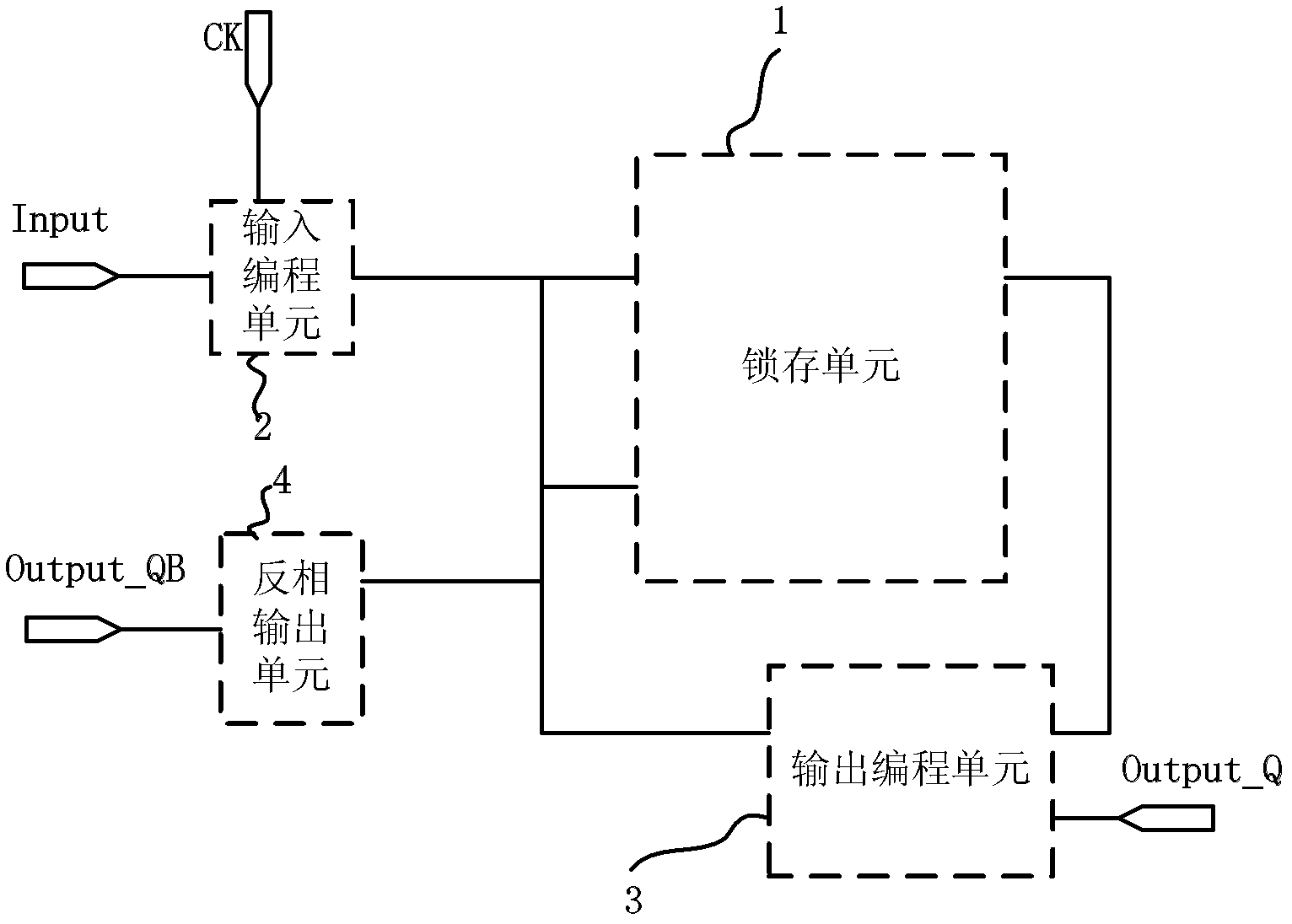
[0050] Specifically, the circuit structure of the shift register in Embodiment 1 of the present invention is as follows Figure 4 As shown, the shift register mainly includes a latch unit 1 , an input programming unit 2 , an output programming unit 3 and an inverted output unit 4 . Figure 4 Among them, the latch unit 1 includes a first inverter and a second inverter connected end to end, and the rest of the units are thin film transistors, which provide working voltages from the operating voltage VDD and the digital ground voltage VSS, and receive two mutually inverting Controlled by the clock signals CK and CKB, it simultaneously receives two mutually inverting input signals Input1 and Input2, and outputs two mutually inverting output signals Output_Q and Output_QB.

[0051] exist Figure 4 In the shown embodiment 1, it is exemplified that all the thin film transistors are N-type thin film transistors. The input programming unit 2 includes a first thin film transistor T1, ...

Embodiment 2

[0065] In Embodiment 2 of the present invention, the circuit structure of the shift register is as follows Figure 9 As shown, in the second embodiment, the thin film transistors T1-T7 in the shift register except the latch unit 1 are composed of P-type thin film transistors. compared to Figure 4 In the shown embodiment 1, the connection structure of the latch unit 1, the input programming unit 2, the output programming unit 3, and the inverting output unit 4 in this embodiment 2 is basically the same, and in the embodiment 2, only the two clock signals CK and CKB are exchanged, and the two input signals Input1 and Input2 are also exchanged. The cascade structure of the gate driver formed by the shift register of embodiment 2 and Figure 5 The same, the circuit structure remains unchanged; Figure 6 The timing diagram given is still applicable, but the operation details of each stage are adjusted accordingly according to the type of transistor (it is well known in the art ...


PUM


Abstract

The invention relates to the technical field of a display device, and provides a shift register, a grid driver and a display device. The shift register comprises an input programming unit, a latch unit, an output programming unit and an inverted output unit, wherein the input programming unit is connected with an input end of the latch unit and programs for the input end of the latch unit; the latch unit is used for latching an output signal; the non-inverted and inverted output ends of the latch unit are connected through the output programming unit; the output programming unit is connected with an output end of the latch unit and programs for the output end of the latch unit; and the inverted output unit is connected with an inverted output end of the latch unit and used for generating an inverted output signal of the shift register. In the invention, the signal shift output function is realized by use of one latch unit only; the circuit has simple structure and little signal wiring; and a GOA (Gate Driver on Array) circuit formed by cascading occupies a small area, and the occupation of the display area of the display panel can be further reduced, thus the high resolution and narrow border of the display device are realized.

Description

technical field [0001] The invention relates to the technical field of display devices, in particular to a shift register, a gate driver and a display device. Background technique [0002] In TFT-LCD (Thin Film Transistor-Liquid Crystal Display, Thin Film Transistor-Liquid Crystal Display), each pixel unit has a corresponding thin film transistor on the array substrate, and the gate (Gate) of the thin film transistor is connected to the horizontal scanning line (also known as row scanning line), the drain (Drain) is connected to the data line in the vertical direction, and the source (Source) is connected to the pixel electrode. When the display is displaying, if enough positive voltage is applied to a row of scanning lines in the horizontal direction, all the thin-film transistors in the row will be turned on through the control of the gate of the thin-film transistors, and the pixel electrodes corresponding to the row of thin-film transistors will be turned on. It is conn...

Claims


Application Information

Patent Timeline
Patent Type & Authority Applications(China)
IPC IPC(8): G09G3/20
CPCG09G3/20G09G2310/0267G09G2310/0286G11C19/28
Inventor 青海刚祁小敬
Owner BOE TECH GRP CO LTD
Why Eureka
Try Eureka