Bonding equipment for chips and wafers

A wafer bonding and chip technology, applied in welding equipment, optomechanical equipment, precision positioning equipment, etc., can solve the problems of manipulator offset, pick up and release chip unfavorable force control, etc., to achieve the effect of ensuring measurement accuracy

Inactive Publication Date: 2012-09-12
SHANDONG UNIV OF TECH
View PDF5 Cites 10 Cited by
  • Summary
  • Abstract
  • Description
  • Claims
  • Application Information

AI Technical Summary

Problems solved by technology

[0004] In the chip and wafer-level packaging process, the operator is a common part in the chip pick-up and release process, which is usually in the shape of a cantilever, such as the operator in the application CN2011202798...

Method used


Image

  • Bonding equipment for chips and wafers
  • Bonding equipment for chips and wafers
  • Bonding equipment for chips and wafers

Examples


Embodiment Construction

[0019] Hereinafter, specific implementation manners of the present invention will be described in detail with reference to the accompanying drawings.

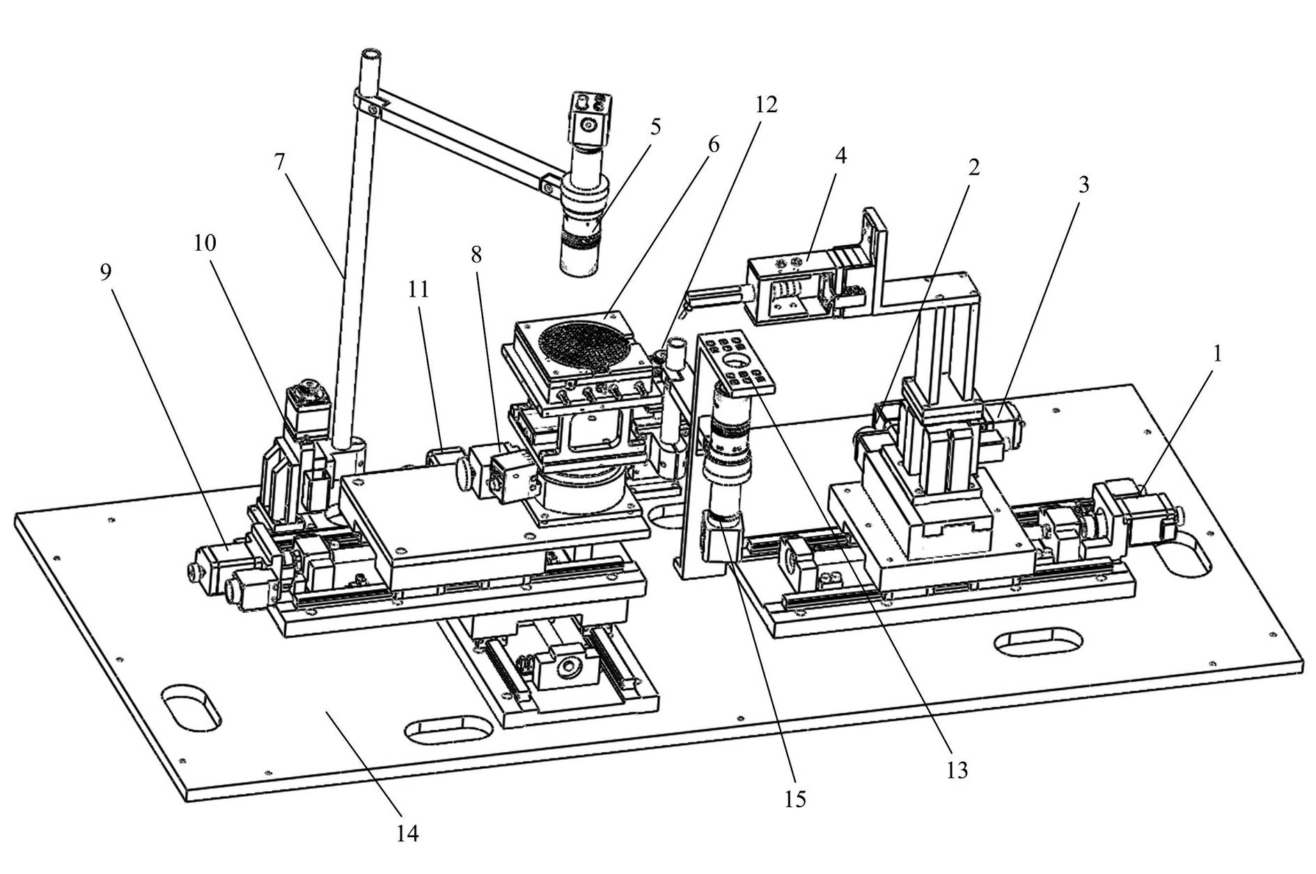
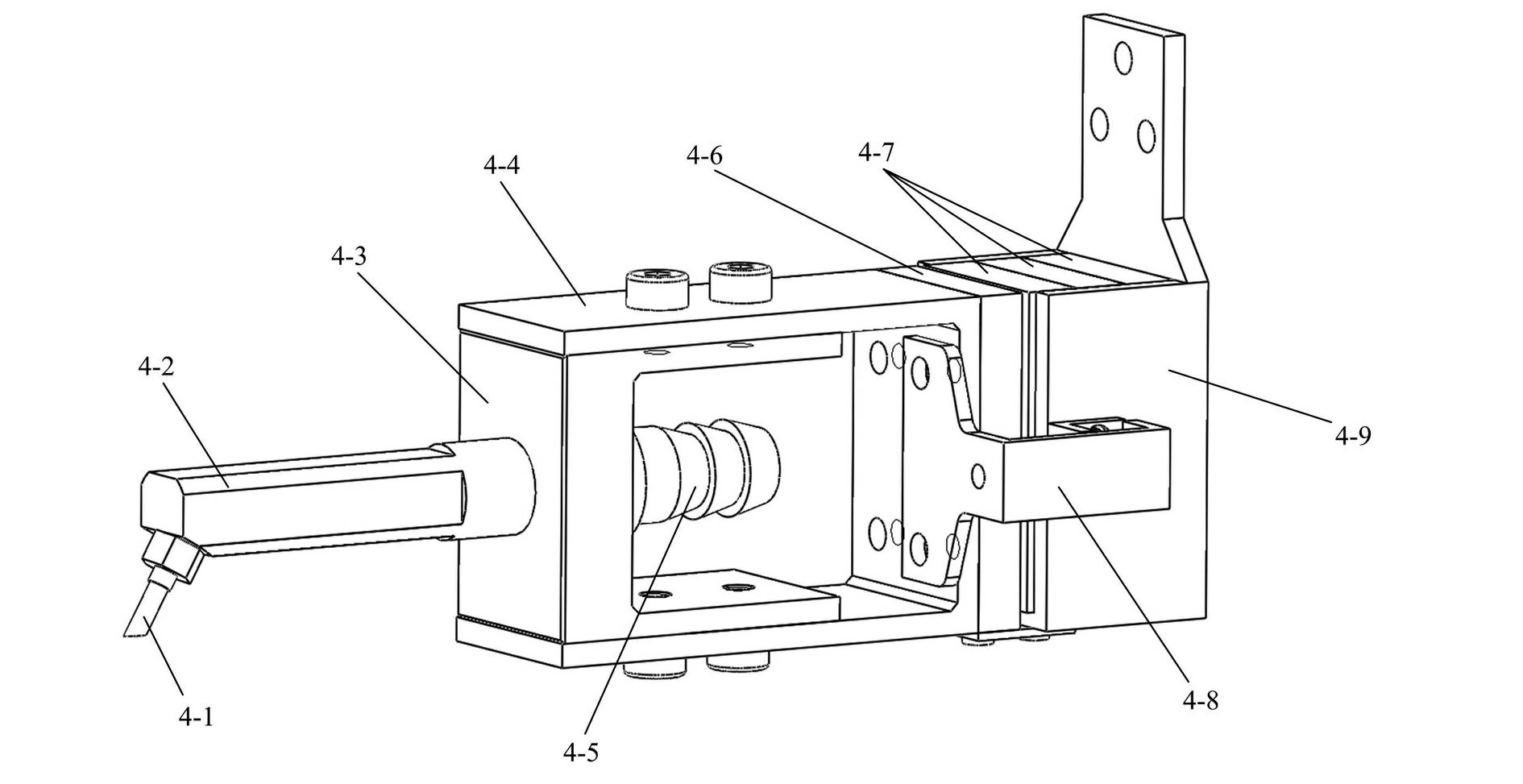
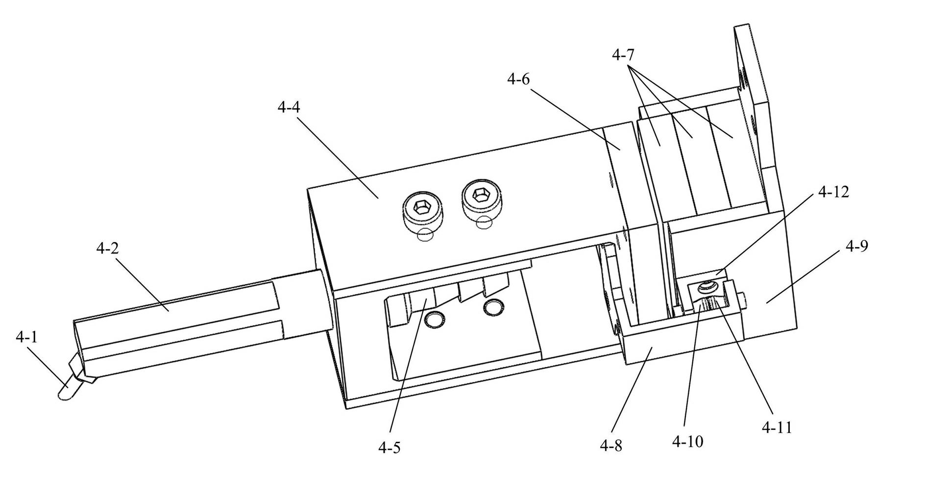
[0020] figure 1 It is a structural diagram of the chip and wafer bonding equipment of the present invention. Such as figure 1 As shown, the bonding equipment is installed on the bottom plate 14, including the wafer stage 6, the storage assembly 13, the operator 4, the microscopic system and the external control system ( figure 1 not shown). The wafer table 6 is used to fix a wafer, and is also a working carrier during bonding. A heating device is arranged on the wafer table 6, and the heating device is used to heat the chip and the wafer to the bonded state during the bonding process. to the desired temperature. The storage component 13 is used to store multiple chips, and the multiple chips may be of the same type or of different types. The operating hand 4 is used to pick up a chip from the storage component 13, and tran...


PUM


Abstract

The invention discloses bonding equipment for chips and wafers. The bonding equipment comprises a wafer table, a memory module, a manipulator, microscope systems and a control system. Accurate positioning is realized by adopting a motor module with multiple degrees of freedom; the poses of the chips are identified and detected through the microscope systems; the chips are picked and released by the vacuum absorption manipulator; then, applied pressure is measured through piezoelectric ceramics integrated at the rear end of the manipulator, thus, the operation precision is ensured and the proper bonding pressure is applied during the chip operation process. The end faces of two induction copper pillars are contacted with each other, thus, a vacuum sucker is prevented from naturally inclining downwards under the action of gravity, and the measurement accuracy is ensured. Moreover, the position of the vacuum sucker is induced through the two induction copper pillars, thus, the control system is informed to start to detect current output by the piezoelectric ceramics.

Description

technical field [0001] The invention relates to a bonding device for a chip and a wafer, in particular to a bonding device which can be adapted to various chips. Background technique [0002] The difference between Micro-Electro-Mechanical Systems (MEMS) devices and integrated circuits mainly includes two aspects. One is to contain movable structures, and the other is to interact with the environment. These two points bring great difficulty to packaging. , and its high packaging cost is mainly caused by these two points. Due to the movable structure, the movable structure must be protected from damage during the packaging process, so the mature integrated circuit packaging process cannot be directly used. Due to the interaction with the environment, the packaging must not only take into account the interaction with the environment, but also ensure that the performance of the device is not affected, which is very difficult to deal with. At the same time, the pre-alignment b...

Claims


Application Information

Patent Timeline
IPC IPC(8): B81C3/00
Inventor 刘曰涛魏修亭肖春雷孙立宁陈立国
Owner SHANDONG UNIV OF TECH
Why Eureka
Try Eureka