Active photoelectric marking method for MEMS infrared light supply array

An infrared light source and photoelectric identification technology, applied in the field of photoelectric identification, can solve the problems of inability to meet all-weather work requirements, small reflected light field of view, low recognition efficiency, etc., and meet all-weather work requirements, high electro-optical conversion efficiency, and recognition efficiency high effect

Active Publication Date: 2012-09-12
ZHONGBEI UNIV
View PDF4 Cites 7 Cited by
  • Summary
  • Abstract
  • Description
  • Claims
  • Application Information

AI Technical Summary

Problems solved by technology

[0003] In order to solve the problems that the existing photoelectric marking technology is greatly affected by the external environment, cannot meet the requirements of all-weather work, cannot be used for invisible marking under asymmetrical conditions, has low recognition efficiency, and has a small range of reflected light field of view, it provides a MEMS infrared light source array active photoelectric marking method

Method used


Image

  • Active photoelectric marking method for MEMS infrared light supply array
  • Active photoelectric marking method for MEMS infrared light supply array
  • Active photoelectric marking method for MEMS infrared light supply array

Examples


Embodiment 1

[0016] MEMS infrared light source array active photoelectric identification method, the method is realized by the following steps:

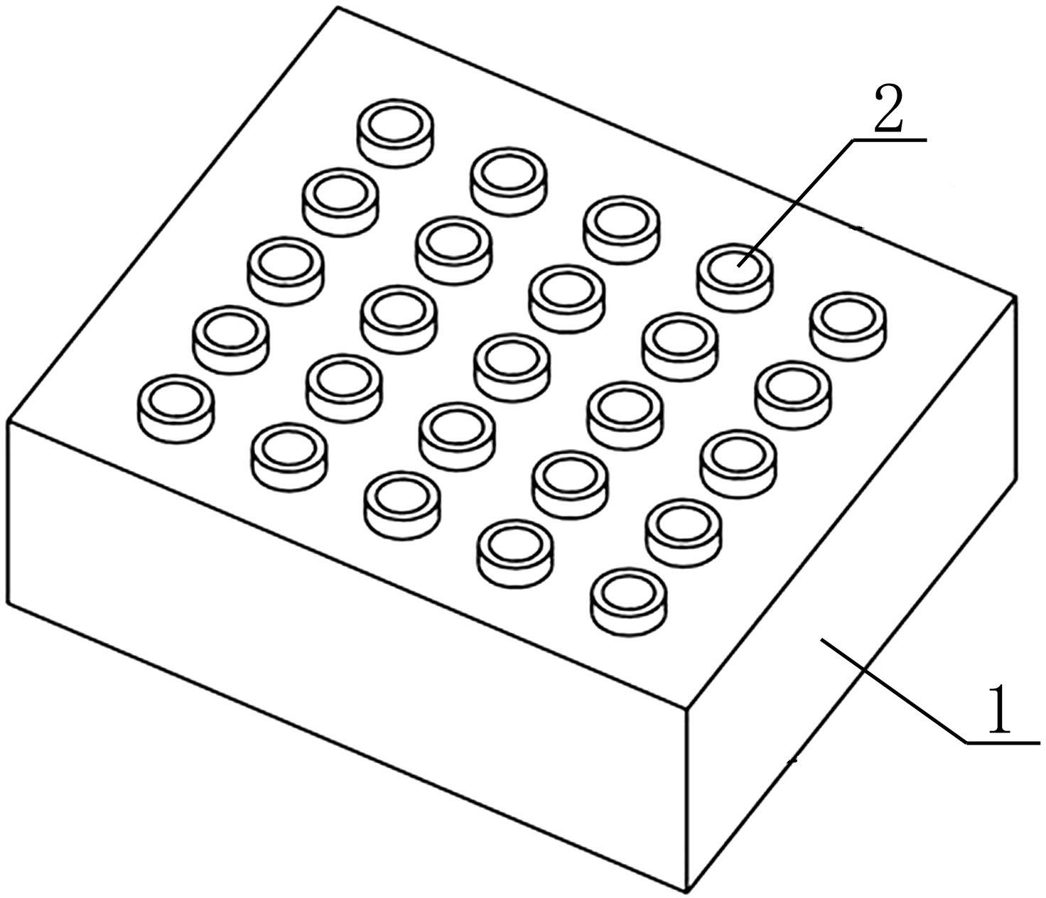
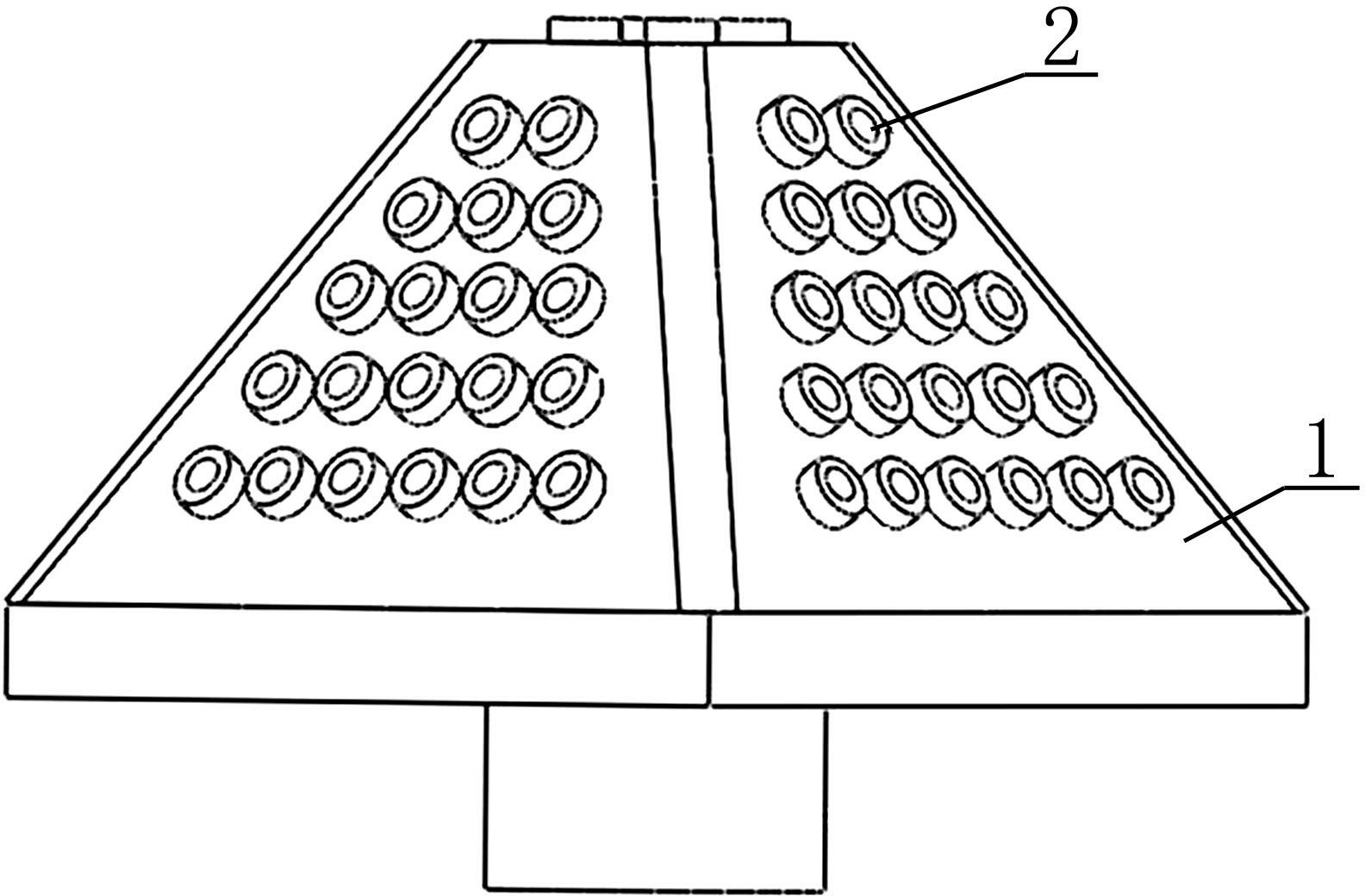
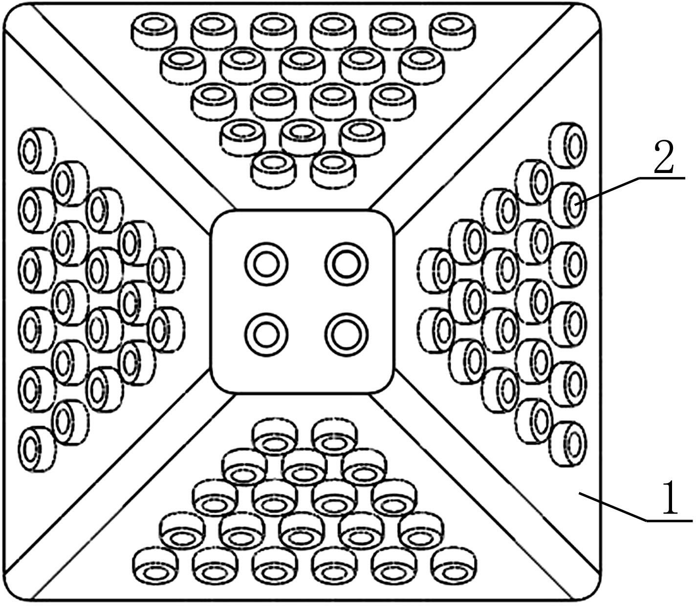
[0017] a. Making an infrared light source array module: select the base 1 and several MEMS infrared light sources 2, and arrange each MEMS infrared light source 2 on the surface of the base 1 to form an infrared light source array; the base 1 and each MEMS infrared light source 2 are shared Form infrared light source array module;

[0018] b. Point radiation source beacon detection: such as Figure 4 As shown, the active point light source photoelectric marking system is formed by FPGA, driving power supply, and infrared light source array module, and the active point light source photoelectric marking system is installed on the beacon; the driving power is each MEMS infrared light source in the infrared light source array module 2Provide driving voltage; FPGA controls the driving voltage output by the driving power supply to control the radiation of ...

Embodiment 2

[0024] MEMS infrared light source array active photoelectric identification method, the method is realized by the following steps:

[0025] a. Making an infrared light source array module: select the base 1 and several MEMS infrared light sources 2, and arrange each MEMS infrared light source 2 on the surface of the base 1 to form an infrared light source array; the base 1 and each MEMS infrared light source 2 are shared Form infrared light source array module;

[0026] b. Point radiation source beacon detection: such as Figure 4 As shown, the active point light source photoelectric marking system is formed by FPGA, driving power supply, and infrared light source array module, and the active point light source photoelectric marking system is installed on the beacon; the driving power is each MEMS infrared light source in the infrared light source array module 2Provide driving voltage; FPGA controls the driving voltage output by the driving power supply to control the radiation of ...


PUM


Abstract

The invention relates to a photoelectric marking technology, in particular to an active photoelectric marking method for an MEMS (Micro-electromechanical Systems) infrared light supply array. The invention solves the problem that the conventional photoelectric marking technology is greatly impacted by external environment, cannot meet the requirements of all-weather work, cannot be used for invisible marking under an asymmetrical condition, is low in identifying efficiency, and is small in the range of a reflected light viewing field. The active photoelectric marking method for the MEMS infrared light supply array is achieved by adopting the following steps: a, an infrared light supply array module is manufactured; b, the radiation signals of an FPGA (Field Programmable Gata Array), used for controlling the infrared light supply array module, are simple point infrared spot signals; and c, the radiation signals of the FPGA, used for controlling the infrared light supply array module, are cyclic switching raster graphic signals. The active photoelectric marking method for the MEMS infrared light supply array, provided by the invention, is applicable to the fields of airplane falling guidance, pilotage, routing indication, bridge marking, personnel search and rescue, subaerial space wireless communication, identification and tracking of military targets, and the like.

Description

Technical field [0001] The invention relates to photoelectric identification technology, in particular to a MEMS infrared light source array active photoelectric identification method. Background technique [0002] Photoelectric marking technology is widely used in the fields of aircraft landing guidance, ship piloting, route marking, bridge marking, urban road marking, personnel search and rescue, and the identification and tracking of military targets. The existing photoelectric marking technology is mainly divided into visible light LED marking technology and passive reflective marking technology. The visible light LED marking technology is currently mainly used in the fields of aircraft landing guidance, ship piloting, and urban road markings. Its core component is the visible light LED (Light Emitting Diode, light-emitting diode) beacon light. The visible light LED beacon light is a solid-state cold light source based on a semiconductor PN junction. Its working principle is...

Claims


Application Information

Patent Timeline
Patent Type & Authority Applications(China)
IPC IPC(8): G01J5/00G01J5/08
Inventor 丑修建熊继军张文栋刘俊田英关新锋李佩青
Owner ZHONGBEI UNIV
Why Eureka
Try Eureka