Method of improving write-in redundancy of static random access memory

A static random, write redundant technology, applied in semiconductor/solid-state device manufacturing, electrical components, circuits, etc., can solve the problem that the static random memory write redundancy is not particularly ideal, and achieve threshold voltage rise, increase The effect of large equivalent resistance and reduced turn-on current

Inactive Publication Date: 2012-09-12
SHANGHAI HUALI MICROELECTRONICS CORP
View PDF3 Cites 0 Cited by
  • Summary
  • Abstract
  • Description
  • Claims
  • Application Information

AI Technical Summary

Problems solved by technology

[0004] However, the writing redundancy of the SRAM manufactured by the SRAM manufacturing method according to the prior art is not particularly ideal, so it is desired to provide a method for effectively improving the writing redundancy of the SRAM

Method used


Image

  • Method of improving write-in redundancy of static random access memory
  • Method of improving write-in redundancy of static random access memory
  • Method of improving write-in redundancy of static random access memory

Examples


Embodiment Construction

[0020] In order to make the content of the present invention clearer and easier to understand, the content of the present invention will be described in detail below in conjunction with specific embodiments and accompanying drawings.

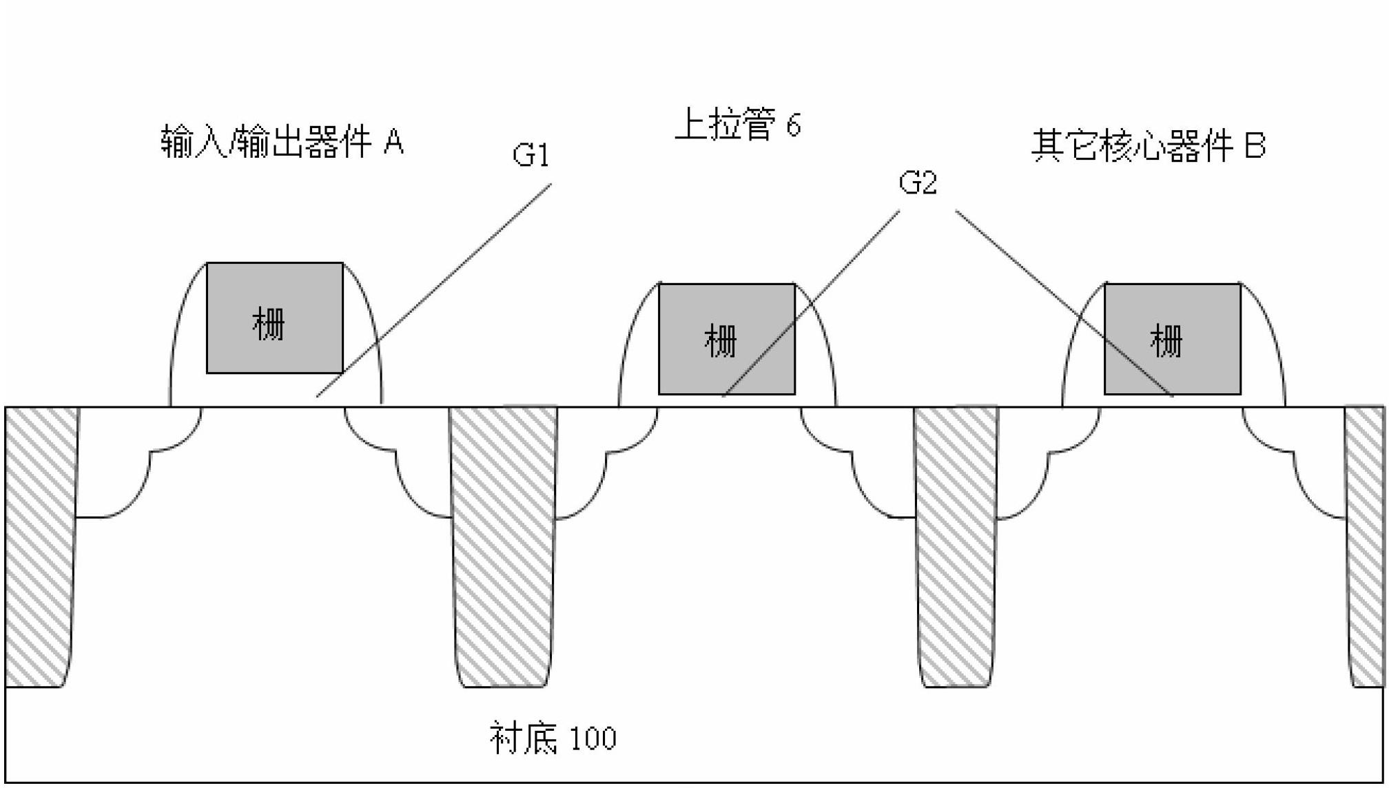
[0021] In the CMOS logic device process, there are usually two main devices, the input / output device (I / O device) and the core device (Core device). The input / output device is mainly used for signal input and output of the chip and peripheral circuits; due to the input I / O devices need to withstand higher voltages, so the gate oxide layer of I / O devices is usually thicker. The core device is mainly used for logic operations inside the chip, etc., and because it needs to be faster, the gate oxide layer of the core device is usually thinner. That is, the gate oxide of the I / O device is typically thicker relative to the core device.

[0022] Likewise, SRAM includes I / O devices as well as core devices.

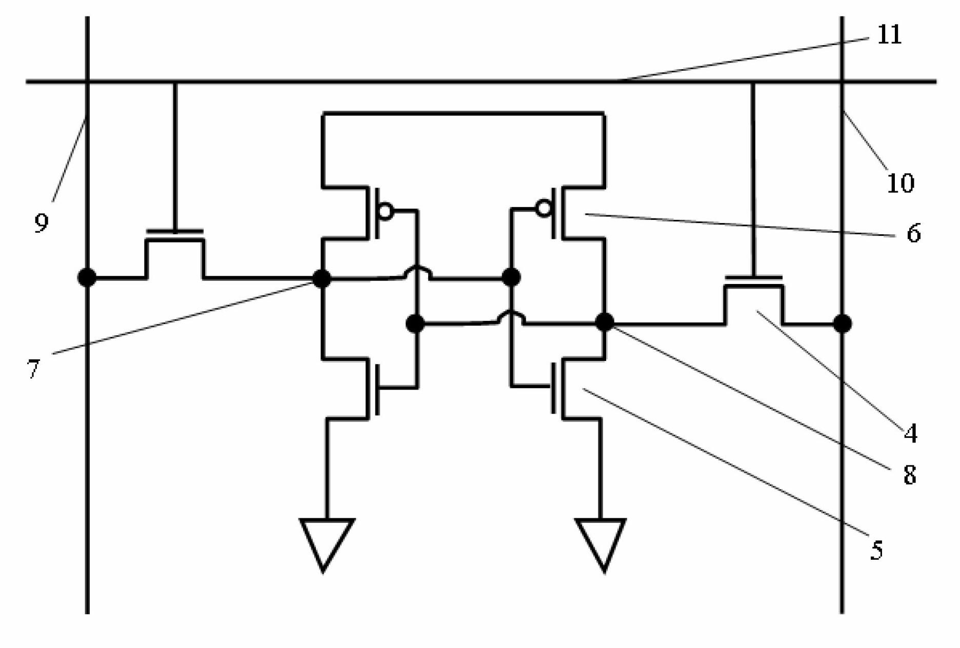
[0023] In particular, for the pull-up trans...


PUM


Abstract

The invention provides a method of improving write-in redundancy of a static random access memory. The static random access memory comprises an input / output device and a core device, wherein the core device comprises a pull-up pipe device, the input / output device is used for inputting and outputting signals of a chip and a peripheral circuit, and the thickness of a grid electrode oxide layer of the input / output device is larger than that of the grid electrode oxide layer of the core device. The method of improving write-in redundancy of static random access memory comprises the step of: enabling the thickness of the grid electrode oxide layer of the pull-up pipe device to be larger than that of the grid electrode oxide layer of the core device, and enabling the thickness of the grid electrode oxide layer of the pull-up pipe device to be equal to that of the grid electrode oxide layer of the core device. For example, when the grid electrode oxide layer of the pull-up pipe device is prepared, the formerly generated grid electrode oxide layer for the input / output device is not moved so as to enable the grid electrode oxide layer of the input / output device to serve as the grid electrode oxide layer of the pull-up pipe device.

Description

technical field [0001] The present invention relates to the technical field of semiconductor preparation, more precisely, the present invention relates to a method for improving the writing redundancy of SRAM, and the manufacture of SRAM using the method for improving the writing redundancy of SRAM method. Background technique [0002] Static random access memory (SRAM), as an important product in semiconductor memory, has been widely used in high-speed data exchange systems such as computers, communications, and multimedia. figure 1 What is shown is a layout structure of a common SRAM cell below 90 nanometers, including three levels of active regions, polysilicon gates, and contact holes. The area 1 marked in the figure is the control transistor (Pass Gate), which is an NMOS device, and the area 2 marked is the pull-down transistor (Pull Down MOS), which is also an NMOS device, and the area 3 is marked The one that comes out is the pull-up tube (Pull Up MOS), and the devi...

Claims


Application Information

Patent Timeline
Patent Type & Authority Applications(China)
IPC IPC(8): H01L21/8244
Inventor 俞柳江
Owner SHANGHAI HUALI MICROELECTRONICS CORP
Why Eureka
Try Eureka