
Method for improving static random access memory reading redundancy

A static random and memory technology, which is applied in semiconductor/solid-state device manufacturing, electrical components, circuits, etc., can solve the problem of low readout performance of random access memory, and achieve improved readout redundancy, reduced turn-on current, increased The effect of large parasitic resistance

Active Publication Date: 2014-08-13
SHANGHAI HUALI MICROELECTRONICS CORP
View PDF4 Cites 0 Cited by
  • Summary
  • Abstract
  • Description
  • Claims
  • Application Information

AI Technical Summary

Problems solved by technology

To solve the problem in the prior art, in the layout structure process of the SRAM cell below 45 nanometers, the gate of the NMOS region is pre-implanted with group V elements, and the gate of the PMOS region is pre-implanted with group III elements. As a result, the readout performance of random access memory is not high.

Method used


Image

  • Method for improving static random access memory reading redundancy
  • Method for improving static random access memory reading redundancy
  • Method for improving static random access memory reading redundancy

Examples


Embodiment Construction

[0022] In order to make the technical means, creative features, objectives and effects of the invention easy to understand, the present invention will be further elaborated below in conjunction with specific diagrams.

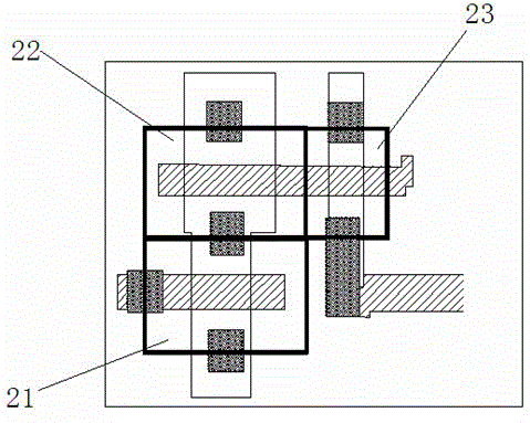
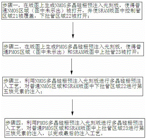
[0023] Such as figure 1 , 2 , Shown in 3, a kind of method for improving SRAM readout redundancy, wherein, comprise following process steps:

[0024] Step 1, generate an NMOS polysilicon gate pre-implantation photoresist on the layout, so that the common NMOS area (not shown in the figure) is opened, and the control tube area 21 in the SRAM layout is covered, and the pull-down tube area 22 is opened;

[0025] Step 2, generate a PMOS polysilicon gate pre-implantation photolithography plate on the layout, so that the pull-up transistor 23 in the common PMOS area (not shown in the figure) and the SRAM layout is turned on;

[0026] Step 3, using the NMOS polysilicon gate pre-implantation photolithography plate to perform the polysilicon gate pre-implantation proc...


PUM


Abstract

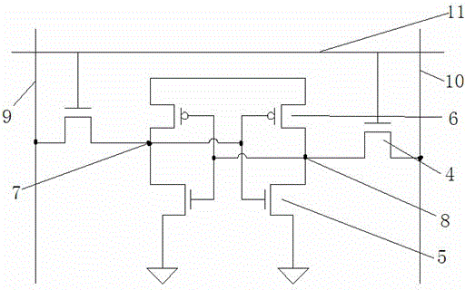
The invention discloses a method for improving static random access memory reading redundancy. The method comprises the following process: through a polycrystalline silicon pre-injection process for removing a control tube; the polycrystalline silicon doping concentration of the control tube is reduced, an equivalent resistance of the control tube is increased, and the random memory reading redundancy is increased. With the adoption of the method for improving static random access memory reading redundancy provided by the invention, the doping concentration of a polysilicon gate of the control tube is reduced effectively without carrying out pre-injection on a control tube area any longer, thereby a parasitic resistance of the polysilicon gate and the polysilicon gate use-up phenomenon are increased, a threshold voltage of the control tube is increased, a starting current is reduced, and at the same time the equivalent resistance of the control tube is increased; and during a reading process, the potential of a node 8 is reduced, thereby increasing the reading redundancy of the random access memory.

Description

technical field [0001] The invention relates to the technical field of semiconductor preparation, in particular to a method for improving the readout redundancy of a static random access memory. Background technique [0002] Static Random Access Memory (SRAM for short), as an important product in semiconductor memory, has been widely used in high-speed data exchange systems such as computers, communications, and multimedia. Such as figure 1 What is shown is a layout structure of a common SRAM cell below 90 nm, including three levels of active regions, polysilicon gates, and contact holes. The area 21 marked in the figure is the control tube (Pass Gate), which is an NMOS area, and the area 22 marked is the pull down tube (Pull Down MOS), which is also an NMOS area, and the area 23 is marked What comes out is the pull-up tube (Pull Up MOS), and this area is a PMOS area. [0003] Read redundancy is an important parameter to measure the read performance of SRAM cells, such as...

Claims


Application Information

Patent Timeline
Patent Type & Authority Patents(China)
IPC IPC(8): H01L21/8244H01L21/265
Inventor 俞柳江
Owner SHANGHAI HUALI MICROELECTRONICS CORP
Learn More