Scan signal line driver circuit and display apparatus having same
A technology for scanning signal lines and driving circuits, applied in the connection/interface layout of logic circuits, logic circuits, electrical components, etc., to solve problems such as inability to transmit video signals
- Summary
- Abstract
- Description
- Claims
- Application Information
AI Technical Summary
Problems solved by technology
Method used
Image


Examples
no. 1 approach >
[0152]
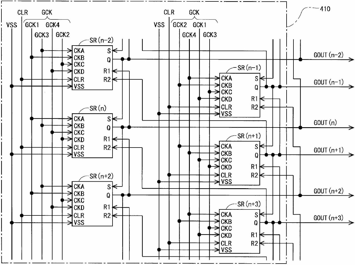
[0153] Figure 4 It is a block diagram showing the overall configuration of the active matrix liquid crystal display device according to the first embodiment of the present invention. Such as Figure 4 As shown, the liquid crystal display device includes: a power supply 100; a DC / DC converter 110; a display control circuit 200; a source driver (video signal line driving circuit) 300; a gate driver (scanning signal line driving circuit) 400; a drive circuit 500 ; and a display section 600 . In addition, the gate driver 400 is formed on a display panel including the display unit 600 using amorphous silicon, polycrystalline silicon, microcrystalline silicon, oxide semiconductor (for example, IGZO), or the like. That is, in the present embodiment, the gate driver 400 has a monolithic structure.
[0154] The display unit 600 includes: multiple (j) source bus lines (video signal lines) SL1˜SLj; multiple (i) gate bus lines (scanning signal lines) GL1˜Gli; and these sour...
no. 2 approach >
[0198]
[0199] Figure 15 It is a block diagram showing a schematic configuration of a shift register in a liquid crystal display device according to a second embodiment of the present invention. In addition, the overall structure of the liquid crystal display device is the same as that of the above-mentioned first embodiment, so the description thereof will be omitted (see Figure 4 ). In the above-mentioned first embodiment, the gate driver 400 includes two shift registers, but in this embodiment, the gate driver 400 includes three shift registers (the first shift register 421, the second shift register 422 and the third shift register 423). That is, if Figure 15 As shown, the entire shift register 420 for driving the gate bus lines GL1 to GLi in the display unit 600 one by one is realized by the first shift register 421 , the second shift register 422 and the third shift register 423 .
[0200] Same as the first embodiment above, each bistable circuit is provided wi...
PUM
 Abstract
Description
Claims
Application Information