Optoelectronic component and method for producing an opto-electronic component

An optoelectronic device and optoelectronic technology, which is applied in the direction of electric solid-state devices, laser components, and structural details of semiconductor lasers, can solve problems such as insufficient realization, high assembly cost, and high cost.

Active Publication Date: 2012-09-12
OSRAM OPTO SEMICONDUCTORS GMBH & CO OHG
View PDF16 Cites 13 Cited by
  • Summary
  • Abstract
  • Description
  • Claims
  • Application Information

AI Technical Summary

Problems solved by technology

[0011] However, the layers deposited by the above commonly used methods have, for example, the disadvantage that with this method only an insufficiently uniform coverage of steep and locally unevenly shaped side walls on all sides can be achieved.
The disadvantages of this method are, on the one hand, the high assembly complexity associated with additional costs and, on the other hand, the inability to prevent damage caused by leaks in the housing and / or residual moisture in the housing. Damage to the laser diode and thus the risk of failure of the laser diode
[0014] Expensive and often insufficient measures of encapsulating the laser diode in a hermetically sealed housing in order to thereby increase the stability of the component have additional, significant disadvantages which are related to the limited structural shape and size. The compactness is associated with the low flexibility regarding the integration of other optical components

Method used


Image

  • Optoelectronic component and method for producing an opto-electronic component
  • Optoelectronic component and method for producing an opto-electronic component
  • Optoelectronic component and method for producing an opto-electronic component

Examples


Embodiment Construction

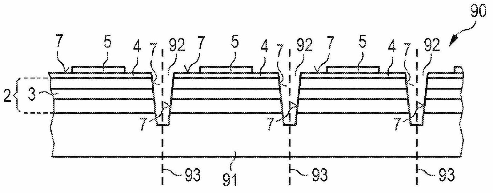
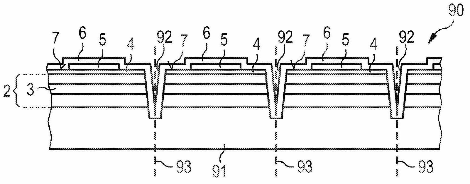
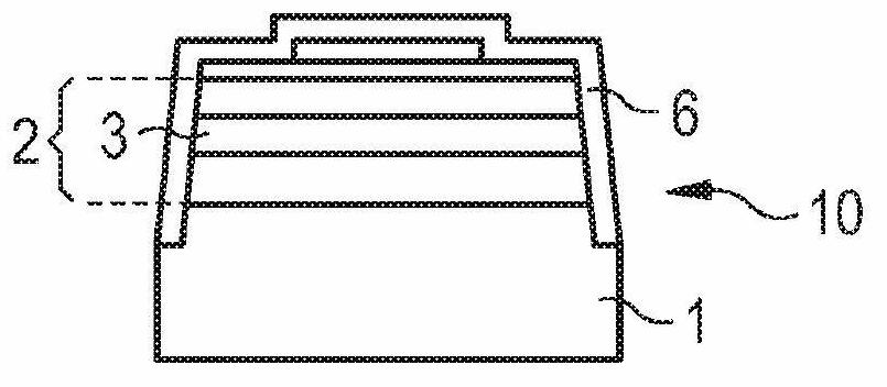
[0060] exist Figures 1A to 1D A method for producing an optoelectronic component 100 having a semiconductor component 10 is shown according to an exemplary embodiment.

[0061] in accordance with Figure 1AIn a first method step, a so-called semiconductor layer assemblage 90 is provided in the form of a so-called wafer assemblage. The semiconductor layer composition 90 has a semiconductor wafer 91 on which the semiconductor layer sequence 2 with the active region 3 is deposited. An electrical contact layer 4 made of metal, a metal layer sequence and / or a metal alloy is applied on the semiconductor layer sequence 2 . In the exemplary embodiment shown, the electrical contact layer 4 is shown purely by way of example and can also be structured, for example. Furthermore, one or more further electrical contact layers can be applied, so that double-sided contacting of the semiconductor layer sequence 2 and in particular double-sided contacting of the active region 3 is possible....


PUM


Abstract

The invention relates to an optoelectronic component comprising at least one inorganic optoelectronically active semiconductor component (10) having an active region (3) suitable for emitting or receiving light during operation, and a sealing material (6) applied to at least one surface region (7) by means of atomic layer deposition, covering the surface region (7) in a hermetically sealing manner. The invention further relates to a method for producing an opto-electronic component.

Description

technical field [0001] The invention proposes an optoelectronic component and a method for producing an optoelectronic component. Background technique [0002] Optoelectronic semiconductor devices such as light-emitting diodes (LEDs), edge-emitting lasers, vertical-cavity surface-emitting lasers (VCSELs), laser arrays, photodiodes, solar cells, phototransistors, etc. are increasingly used in lighting technology, projection, Central components in data storage, printing technology, energy harvesting and many other applications. [0003] Material systems based on AlInGaN, InGaAlP and AlGaAs can cover the entire spectral range from ultraviolet to infrared for emitting or detecting semiconductor devices. Light sources based in particular on so-called semiconductor systems have advantages over competing solutions such as incandescent lamps or halogen light sources in terms of their compactness and high service life. [0004] In this case, innovative technical developments, such ...

Claims


Application Information

Patent Timeline
Patent Type & Authority Applications(China)
IPC IPC(8): H01L33/44H01L31/0216
CPCH01L24/24H01L24/48H01L24/82H01L33/0095H01L2224/24145H01L2224/24226H01L2224/48091H01L2224/48227H01L2224/484H01L2224/8592H01L2924/01004H01L2924/01012H01L2924/01013H01L2924/01014H01L2924/0102H01L2924/01031H01L2924/01032H01L2924/01038H01L2924/01058H01L2924/01073H01L2924/01078H01L2924/01082H01L2924/10329H01L2924/10336H01S5/02H01S5/20H01S2301/176H01L2924/01005H01L2924/01023H01L2924/01033H01L2924/0104H01L2924/01068H01L2924/01072H01L2924/014H01L2924/12041H01L2924/3025H01L2924/00014H01L2924/12042H01L2924/12036H01L2924/12043H01L2924/181H01L2933/0025H01L31/02005H01L31/035281H01L33/44H01L31/0203H01L31/02161H01L2924/00H01L2224/45099H01L2924/00012H01L2224/85399H01L2224/05599H01L31/02019H01L31/186H01L33/56H01L33/62H01L2933/005H01S5/028
Inventor 艾尔弗雷德·莱尔迈克尔·费雷尔蒂尔曼·施伦克尔森克·陶茨乌韦·施特劳斯马丁·穆勒
Owner OSRAM OPTO SEMICONDUCTORS GMBH & CO OHG
Why Eureka
Try Eureka