Anisotropic conducting film and method for producing same

An anisotropic, conductive film technology, applied in the fields of printed circuit manufacturing, cable/conductor manufacturing, semiconductor/solid device manufacturing, etc., can solve problems such as difficult to uniformly install electronic components, multiple workloads, SMD misalignment, etc., to achieve capture Improved effect

Inactive Publication Date: 2012-09-12
DEXERIALS CORP
View PDF6 Cites 4 Cited by
  • Summary
  • Abstract
  • Description
  • Claims
  • Application Information

AI Technical Summary

Problems solved by technology

In addition, the mounting of SMD201 requires individual temporary mounting (temporary pasting), which requires a considerable amount of work.
[0009] In addition, although it is conceivable to use the same ACF to mount SMD, FPC, and IC at the same time, it is difficult to uniformly mount these electronic components with high precision because the ACF characteristics required for SMD, FPC, and IC are different.
For example, when temporarily mounting a small SMD such as a capacitor on an ACF for COG (adhesion: 5 to 80kPa), as in Figure 8 shown, misalignment of the SMD will occur

Method used


Image

  • Anisotropic conducting film and method for producing same
  • Anisotropic conducting film and method for producing same
  • Anisotropic conducting film and method for producing same

Examples


Embodiment

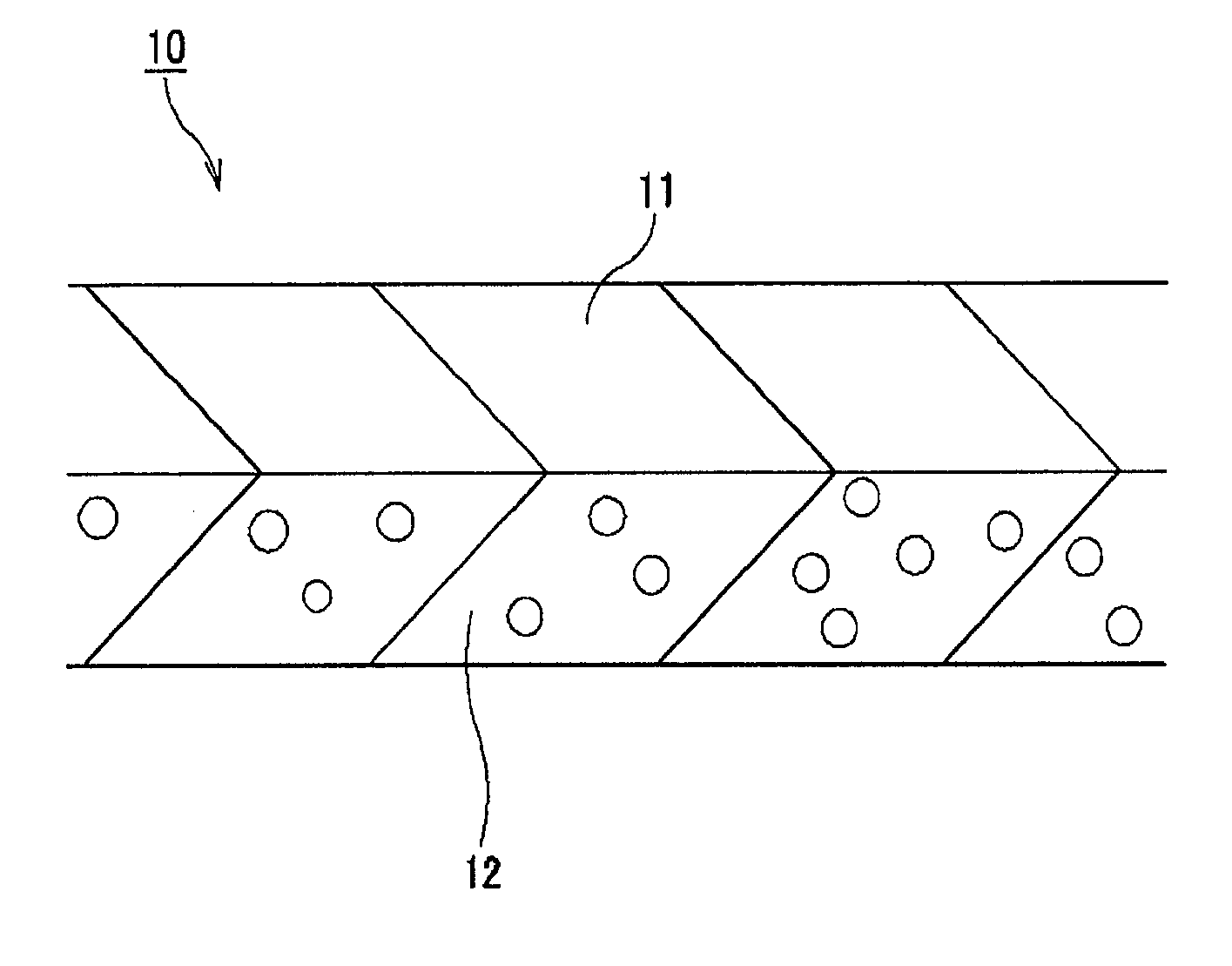
[0050] Embodiments of the present invention are described below. First, according to the mixing ratio shown in Table 1, phenoxy resin, liquid epoxy resin, latent curing agent, silane coupling agent, silicon particles and conductive particles were dissolved in toluene, and the solution was applied on the peeling surface. On the film, a predetermined dry thickness was formed, and after drying in an oven, resins A to G were produced.

[0051] In Table 1, "PKHH" is a phenoxy resin manufactured by Phenoxy Corporation. In addition, 'EP828' is a bisphenol A type liquid epoxy resin manufactured by Japan Epoxy Corporation. In addition, 'HX3941' is a microcapsule-type imidazole latent curing agent manufactured by Asahi Kasei Chemical Co., Ltd. In addition, 'A-187' is an epoxy-based silane coupling agent manufactured by Momentive Paphormans Materials Japan Co., Ltd. In addition, 'RY200' is a hydrophobic silicon particle manufactured by Nippon Aerosil Co., Ltd. In addition, 'Ni / Au pla...


PUM

PropertyMeasurementUnit
viscosityaaaaaaaaaa
thicknessaaaaaaaaaa
thicknessaaaaaaaaaa

Abstract

Electronic components of different sizes are simultaneously mounted with high precision. The disclosed film has a two-layer configuration of a first resin layer (11) having a tack strength of at least 200 kPa, and a second resin layer (12) containing conductive particles. By means of electronic components being installed in the first resin layer (11), use on an IC, FPC, and SMD becomes possible, and simultaneous mounting becomes possible.

Description

technical field [0001] The present invention relates to an anisotropic conductive film in which conductive particles are dispersed and a method for producing the same. [0002] This application claims priority based on Japanese Patent Application No. Japanese Patent Application No. 2009-225771 filed on September 30, 2009 in Japan, and by referring to this application, it is incorporated in the present application. Background technique [0003] Until now, when bonding an IC (Integrated Circuit) and other electronic components to a glass substrate, the IC was mounted on a glass substrate (COG: Chip on Glass), and other electronic components were mounted on a flexible printed circuit board (FPC). : Flexible Printed Circuits). [0004] For example, if Figure 6 Like the illustrated liquid crystal device, SMD (Surface Mount Device) 101 such as a capacitor is mounted on FPC 102 , and IC 103 is mounted on glass substrate 104 . In addition, the FPC 102 and the glass substrate 104 ...

Claims


Application Information

Patent Timeline
Patent Type & Authority Applications(China)
IPC IPC(8): H01R11/01H01B5/16H01B13/00H01L21/60H01R43/00
CPCC08K9/02C09J7/10C09J9/02C09J2203/326C09J2301/208C09J2301/408H01L24/29H01L24/83H01L2224/29082H01L2224/29101H01L2224/2919H01L2224/2929H01L2224/29298H01L2224/838H01L2924/00011H01L2924/00013H01L2924/01004H01L2924/01005H01L2924/01006H01L2924/01012H01L2924/01019H01L2924/0102H01L2924/01023H01L2924/01029H01L2924/01033H01L2924/01067H01L2924/01074H01L2924/01078H01L2924/01079H01L2924/014H01L2924/0665H01L2924/0781H01L2924/14H01L2924/15788H01L2924/19041H01R4/04H01R12/62H01R12/7076H05K3/323H05K3/361H05K2203/1189H01L2924/00H01L2224/29099H01L2224/29199H01L2224/29299H01B5/16H01B13/00H01R11/01
Inventor 深谷达朗松岛隆行山本润相崎亮太工藤克哉古田和隆
Owner DEXERIALS CORP
Why Eureka
Try Eureka