
Wiring connection methods and functional devices

A technology for functional devices and connection methods, applied in connection, circuit/collector parts, semiconductor devices, etc., can solve problems such as yield deterioration, and achieve the effects of improving yield, efficient manufacturing, and reliable electrical connection

Inactive Publication Date: 2016-03-02
TOHOKU UNIV
View PDF4 Cites 0 Cited by
  • Summary
  • Abstract
  • Description
  • Claims
  • Application Information

AI Technical Summary

Problems solved by technology

In the surface polishing process of the substrate 103 with a through-hole wiring, there is a problem particularly when the amount of depression on the surface of the through-hole wiring 103a is not constant, resulting in deterioration of the yield.

Method used


Image

  • Wiring connection methods and functional devices
  • Wiring connection methods and functional devices
  • Wiring connection methods and functional devices

Examples


Embodiment 1

[0072] Figure 9 It is a figure which shows the process of the wiring connection method performed in Example 1. The first substrate 70 and the second substrate 75 are fabricated by the following method.

[0073] With regard to the first substrate 70, steps are locally formed on the silicon substrate 71, and after an oxide film is formed by CVD, the oxide film on the surface to be bonded to the second substrate 75 is wet-etched, and on the remaining oxide film 72 A circuit was formed, and a Ti layer 73 a of 100 nm and a Cu layer 73 b of 600 nm were sequentially laminated as the connection electrode portion 73 . The surface of the electrode pad serving as the connection electrode portion 73 was lowered by 300 nm than the bonding surface.

[0074] In the second substrate 75 , a Cr layer 77 a and a Cu layer 77 b are sequentially stacked on the through wiring 76 a of the LTCC substrate 76 as the connection electrode portion 77 , and a Sn layer is stacked as the metal layer 78 . ...

Embodiment 2

[0087] In Example 2, the height of the Sn layer as the metal layer 78 from the bonding surface of the LTCC substrate 76 was 1000 nm. Other than that, it is the same as in Example 1.


PUM


Abstract

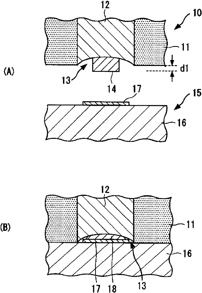
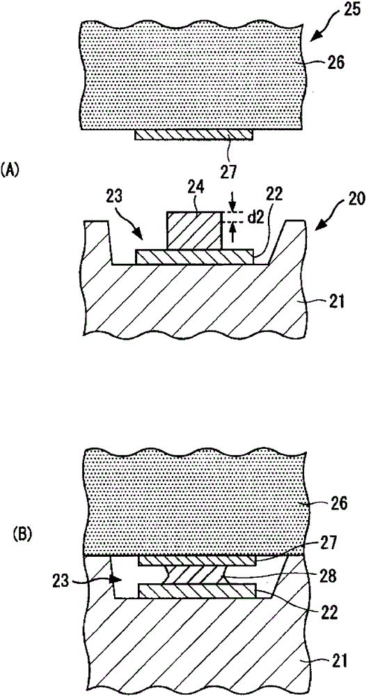
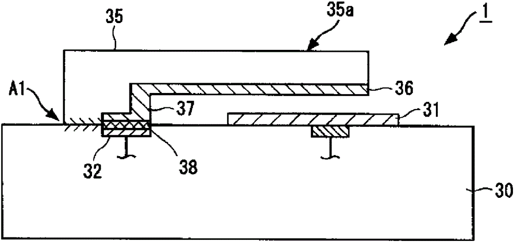
The present invention provides a wiring connection method and a functional device. A metal layer (14) is preliminarily formed on at least one of the connection electrode portion (12) of the first substrate (10) and the connection electrode portion (17) of the second substrate (15) to form the first substrate (10). The connecting electrode portion (12) of the ) and the connecting electrode portion (17) of the second substrate (15) are opposite to each other through the metal layer (14) after the first substrate (10) and the second substrate (15) are overlapped, and then passed A direct current voltage is applied between the first substrate (10) and the second substrate (15) while the temperature of the first substrate (10) and the second substrate (15) is raised to the anodic bonding temperature and the temperature is maintained, and the first substrate (10) ) is anodic-bonded with the second substrate (15), and at the same time, the metal layer (14) is melted to connect the connecting electrode portion (12) of the first substrate (10) and the connecting electrode portion (12) of the second substrate (15). 17) Make electrical connections. Thereby, it is possible to perform anodic bonding of a plurality of substrates with good yield and to perform wiring connection, which is effective for packaging and the like.

Description

technical field [0001] The present invention relates to a wiring connection method capable of electrically connecting substrates when anodic bonding is performed, and a functional device manufactured using the wiring connection method. Background technique [0002] For example, electronic circuits and MEMS structures are sealed by bonding a second substrate such as a glass substrate to a first substrate on which various electronic circuits and MEMS structures (Micro Electro Mechanical Systems: Micro Electro Mechanical Systems) are formed. Specifically, various electronic circuits and MEMS are provided on semiconductor substrates and glass substrates by microfabrication such as thin film manufacturing processes and etching processes. Then, heating is performed in a state where the substrates are overlapped, and a voltage is applied such that a negative voltage is applied to the glass substrate side and a positive voltage is applied to the semiconductor substrate, so that the ...

Claims


Application Information

Patent Timeline
Patent Type & Authority Patents(China)
IPC IPC(8): H01R43/02H01L23/02
CPCB81B2203/04B81C3/001B81C2203/031H01L2924/01004H01L2924/01011H01L2924/01013H01L2924/01027H01L2924/01029H01L2924/01033H01L2924/01049H01L2924/01078H01L2924/01079H01L2924/01327H01L2924/09701H01L2924/14H01R43/0214H01L2924/01005H01L2924/01006H01L2924/01019H01L2924/01023H01L2924/01024H01L2924/01047H01L2924/014H01L2224/81893H01L24/81H01L2224/81192H01L2224/8181H01L2224/97H01L2224/16503H01L2224/16227H01L2224/16225H01L2924/1461H01L2924/15788H01L24/16H01L2924/10253H01L2224/81H01L2924/00
Inventor 田中秀治江刺正喜松崎荣毛利护
Owner TOHOKU UNIV
Learn More