
Intelligent defect screening and sampling method

A defect and intelligent technology, applied in the field of defect analysis, can solve the problems of limited number, omission to identify fatal defects, limited time of the foundry, etc., to achieve the effect of increasing the detection rate

Active Publication Date: 2012-09-19
ELITETECH TECH
View PDF3 Cites 21 Cited by
  • Summary
  • Abstract
  • Description
  • Claims
  • Application Information

AI Technical Summary

Problems solved by technology

However, foundry time is limited, and the performance of scanning electron microscopes used for inspection may limit the number of observations per wafer
Therefore, the current technology has difficulty in identifying important types of defects on the product, and there is a risk of missing the identification of fatal defects
[0004] Without a fast and innovative method to pre-identify systemic defects, foundries will face huge production declines and spend a lot of learning time in mass production

Method used


Image

  • Intelligent defect screening and sampling method
  • Intelligent defect screening and sampling method
  • Intelligent defect screening and sampling method

Examples


no. 1 example 〕

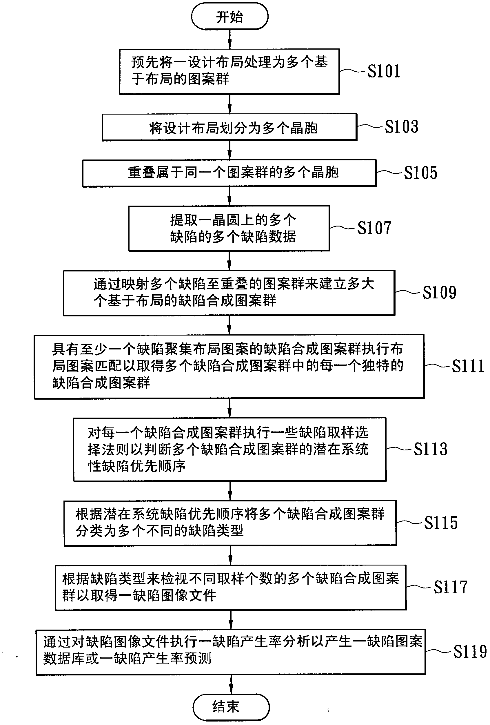
[0036] Next, please refer to Figure 1B , Figure 1B It is a flow chart of the first embodiment of the intelligent defect screening and sampling method of the present invention.

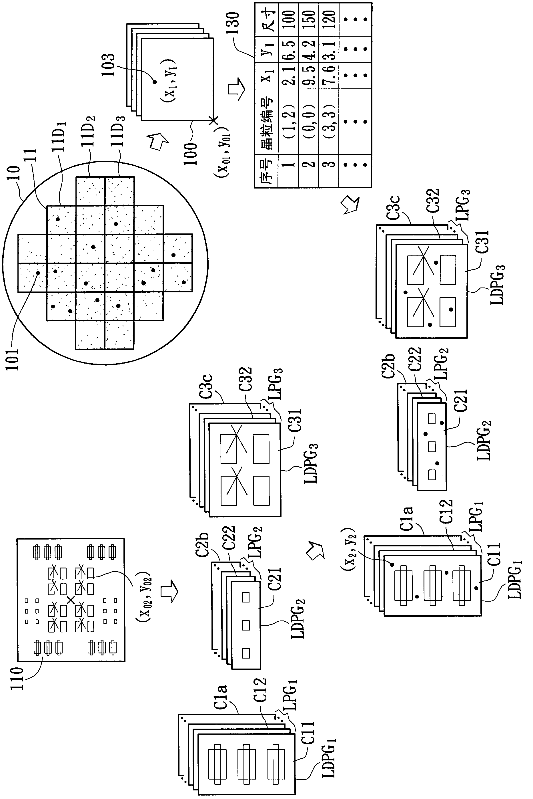
[0037] Please also refer to Figure 1C , Figure 1C It is a schematic diagram of the first embodiment of the intelligent defect screening and sampling method of the present invention.

[0038] The user pre-processes the design layout 110 into a plurality of layout based pattern group (layout based pattern group) LPG 1 、LPG 2 、LPG 3 (S101), wherein the design layout 110 is designed by the user for the wafer 10, the wafer 10 has a full-chip layout (full-chip layout) 11, and the full-chip layout 11 includes a plurality of dies (die) 11D 1 , 11D 2 ,, 11D 3 , extract a plurality of dies 11D from a design layout database by computer 1 , 11D 2 ,, and 11D 3 design layout 110, the extracted design layout 110 has a plurality of layout patterns (layout pattern) and a second reference origin (x O2 ,y...

no. 2 example

[0053] Please refer to figure 2 , figure 2 It is a flow chart of the second embodiment of the intelligent defect screening and sampling method of the present invention. Such as figure 2 As shown, the intelligent defect screening and sampling method of the second embodiment is roughly the same as the intelligent defect screening and sampling method of the first embodiment, the difference is that the computer establishes a plurality of layout-based defect synthesis pattern groups LDPG 1 、LDPG 2 、LDPG 3 After ( S109 ), the intelligent defect screening and sampling method of the second embodiment further includes the following steps.

[0054] The computer-implemented defect sampling selection algorithm consists of calculating the LDPG for each defect composite pattern group 1 、LDPG 2 or LDPG 3 A hit rate (S211). where the hit rate is about each defect synthetic pattern group LDPG 1 、LDPG 2 or LDPG 3 The relationship between the number of multiple defects 101 and the ...

no. 3 example

[0065] Please refer to image 3 , image 3 It is a flow chart of the third embodiment of the intelligent defect screening and sampling method of the present invention. Such as image 3 As shown, the intelligent defect screening and sampling method of the third embodiment is roughly the same as the intelligent defect screening and sampling method of the first embodiment, the difference is that after the computer generates a defect pattern database or a defect generation rate prediction (S119) , The intelligent defect screening and sampling method of the third embodiment further includes the following steps.

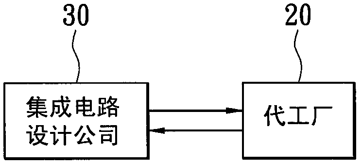
[0066] The design company 30 downloads the defect pattern database from the website of the factory 20 (S321). The user of the design company 30 extracts a new design layout from a design layout database (S323). Pattern matching is performed on a plurality of new design layout patterns of the new design layout and a plurality of layout patterns in the defect database by...


PUM


Abstract

The invention discloses an intelligent defect screening and sampling method, which comprises the following steps of: previously processing a design layout into a plurality of pattern groups based on the layout; dividing the design layout into a plurality of crystal cells; overlapping the crystal cells which belong to the same pattern group; extracting a plurality of pieces of defect data of a plurality of defects on a wafer; mapping a plurality of defects to the overlapped pattern groups to establish a plurality of defect synthesis pattern groups based on the layout; performing layout pattern matching on the defect synthesis pattern groups; performing some defect sampling selection rules on each defect synthesis pattern group to judge a potential systematic defect priority order; classifying the defect synthesis pattern groups into different defect types according to the potential systematic defect priority order; inspecting the defect synthesis pattern groups of different sampling numbers to obtain a defect image file according to the defect types; and performing defect generation rate analysis on the defect image file to generate a defect pattern database or perform defect generation rate prediction. According to the intelligent defect screening and sampling method, the defection rate of systematic defects and defect inspection efficiency can be increased.

Description

technical field [0001] The invention relates to a defect analysis method, and in particular to a defect screening and sampling method. Background technique [0002] The manufacturing process of integrated circuits includes thin film deposition, photomask exposure, photolithography, etching, etc. During the manufacturing process, random particle defects and systematic defects inevitably occur. It will affect the yield rate of the product, and the yield rate of the product is related to the cost of the die. [0003] As the feature size of design layouts shrinks, yield-related defects become smaller. In order to extract all the killer defects on the wafer, the foundry must increase the sensitivity of its scanning and inspection equipment. Therefore, the number of detected defects will also increase, however, in fact, the percentage of non-fatal defects to all detected defects will also increase. In addition, in order to identify the real potential defects, the foundry will us...

Claims


Application Information

Patent Timeline
Patent Type & Authority Applications(China)
IPC IPC(8): H01L21/00
Inventor 吕一云林钦贤
Owner ELITETECH TECH
Learn More