
Large-sensitization area CMOS image sensor pixel structure and generation method thereof

An image sensor and pixel structure technology, applied in the field of pixel structure, can solve the problems of reducing long-wavelength light quantum efficiency, reducing pixel well capacity, etc., and achieve the effects of reducing image noise, increasing injection concentration, and improving well capacity

Inactive Publication Date: 2012-09-19
TIANJIN UNIV
View PDF2 Cites 7 Cited by
  • Summary
  • Abstract
  • Description
  • Claims
  • Application Information

AI Technical Summary

Problems solved by technology

However, reducing the impurity concentration of the N region 2 will reduce the well capacity of the pixel; reducing the distance between the bottom edge of the N region 2 and the oxide layer will reduce the long-wavelength photon efficiency
Therefore, there is a problem of mutual restriction between the area of ​​the clamp diode N region 2, the implantation depth and the dose.

Method used


Image

  • Large-sensitization area CMOS image sensor pixel structure and generation method thereof
  • Large-sensitization area CMOS image sensor pixel structure and generation method thereof
  • Large-sensitization area CMOS image sensor pixel structure and generation method thereof

Examples


Embodiment Construction

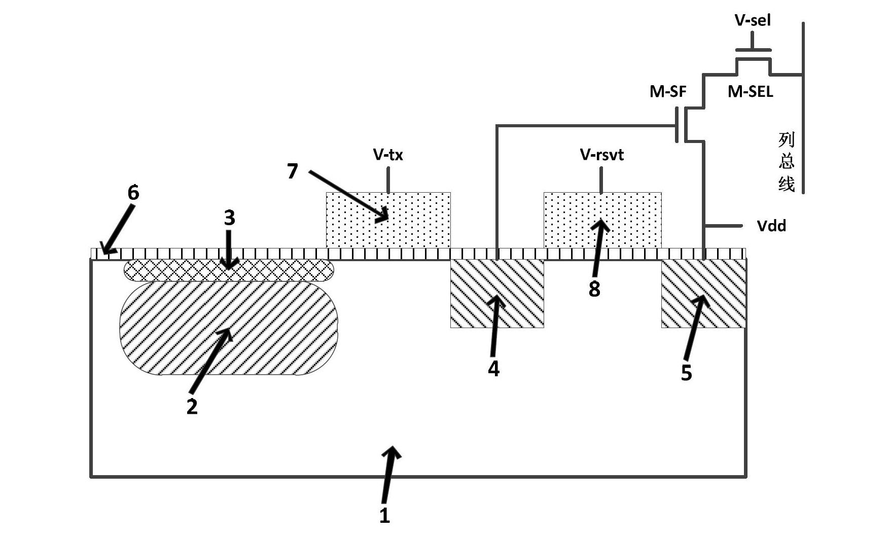
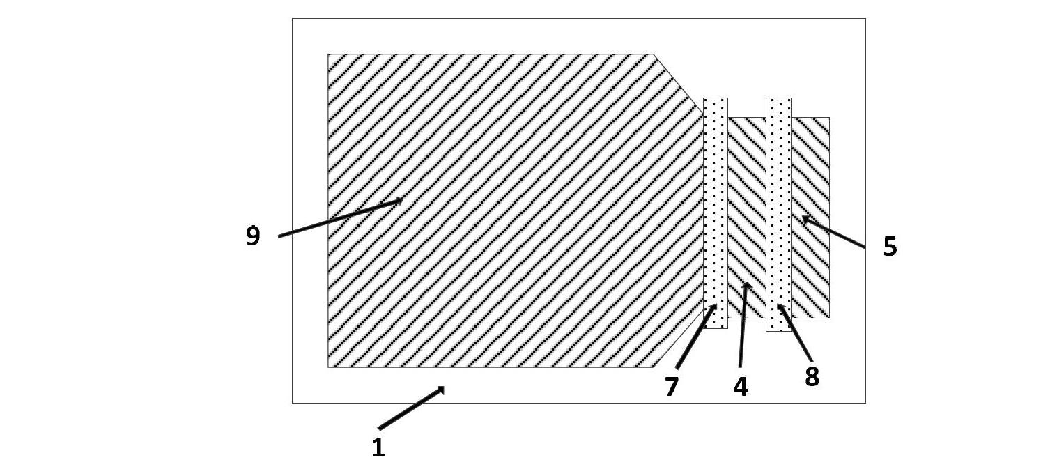
[0023] The technical solution adopted by the present invention is that the pixel structure of the CMOS image sensor with a large photosensitive area is composed of a transmission tube TX, a reset tube RST, a source follower SF, a selection tube SEL, a clamp diode PPD and a storage node FD, and the clamp diode PPD is The N region of the clamp diode and the P region of the clamp diode are arranged on the P-type impurity substrate, and a new P-type impurity injection region is arranged between the N region of the clamp diode and the P region of the clamp diode. The ratio of the area of ​​the overlapping portion of the impurity injection region and the photosensitive region of the clamp diode to the area of ​​the photosensitive region is between 1:100 and 1:5; the shortest distance between the overlapping portion and the TX gate of the transmission tube is greater than 2um; the new P-type impurity The implantation depth of the peak concentration of the implantation region is within...


PUM


Abstract

The invention relates to a solid complementary metal oxide semiconductor (CMOS) image sensor. In order to provide a large pixel structure with excellent property parameter and increase quantum efficiency of pixels to long-wavelength light to acquire a more actual colorful image, the technical scheme adopted by the invention is as follows: a large-sensitization area CMOS image sensor pixel structure and a generation method thereof are provided, a clamp diode PPD is as follows: an N region of the clamp diode and a P region of the clamp diode are arranged on a P type impurity substrate, a new P type impurity injection region is arranged between the N region of the clamp diode and the P region of the clamp diode, and the proportion of the area of an overlapping part of the new P type impurityinjection region and a clamp diode sensitization region to the area of the sensitization region is 1:100-1:5; the shortest distance between the overlapping part and a TX grid of a transmission tube is more than 2 mu m; and the depth of concentration peak injection of the new P type impurity injection region is within an impurity depth distribution range of an N type impurity region. The inventionis mainly applied to the design and the manufacture of the CMOS image sensor.

Description

technical field [0001] The invention relates to the field of solid-state CMOS image sensors, in particular to a pixel structure for improving the quantum efficiency of large-scale pixels. Background technique [0002] In recent years, with the continuous development of the manufacturing process of CMOS integrated circuits, especially the design and manufacturing process of CMOS image sensors, CMOS image sensors have gradually replaced CCD image sensors and become the mainstream. CMOS image sensors have the advantages of higher process integration and lower power consumption. [0003] The traditional 4T-PPD active pixel structure section diagram is as follows figure 1 As shown, including, 1 is the P-type impurity substrate; 2 is the N region of the clamp diode; 3 is the P region of the clamp diode; 4 is the FD (Floating Diffusion) storage node; 5 is the RST transistor (reset transistor) The drain of the drain is connected to the power supply voltage Vdd; 6 is the oxide laye...

Claims


Application Information

Patent Timeline
Patent Type & Authority Applications(China)
IPC IPC(8): H01L27/146
Inventor 姚素英韩立镪孙羽高静徐江涛史再峰
Owner TIANJIN UNIV
Learn More