Method for inhibiting secondary electron emission of microwave component surface by adopting nanostructure plating layer

A technology for secondary electron emission and microwave components, which is applied in nanotechnology, coating, sputter plating, etc., can solve the problems of poor conductivity of the oxide film and unfavorable microwave signal transmission, etc., and achieve the improvement of discharge threshold and secondary electron emission Coefficient reduction, the effect of reducing the secondary electron emission coefficient

Inactive Publication Date: 2012-10-17
XI AN JIAOTONG UNIV +1
View PDF2 Cites 10 Cited by
  • Summary
  • Abstract
  • Description
  • Claims
  • Application Information

AI Technical Summary

Problems solved by technology

However, the conductivity of the oxide film itself is poor, which is not conducive to the transmission of microwave signals, so the problem of conductivity needs to be solved

Method used


Image

  • Method for inhibiting secondary electron emission of microwave component surface by adopting nanostructure plating layer
  • Method for inhibiting secondary electron emission of microwave component surface by adopting nanostructure plating layer
  • Method for inhibiting secondary electron emission of microwave component surface by adopting nanostructure plating layer

Examples


Embodiment Construction

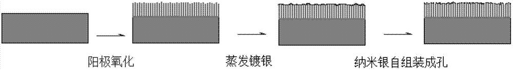
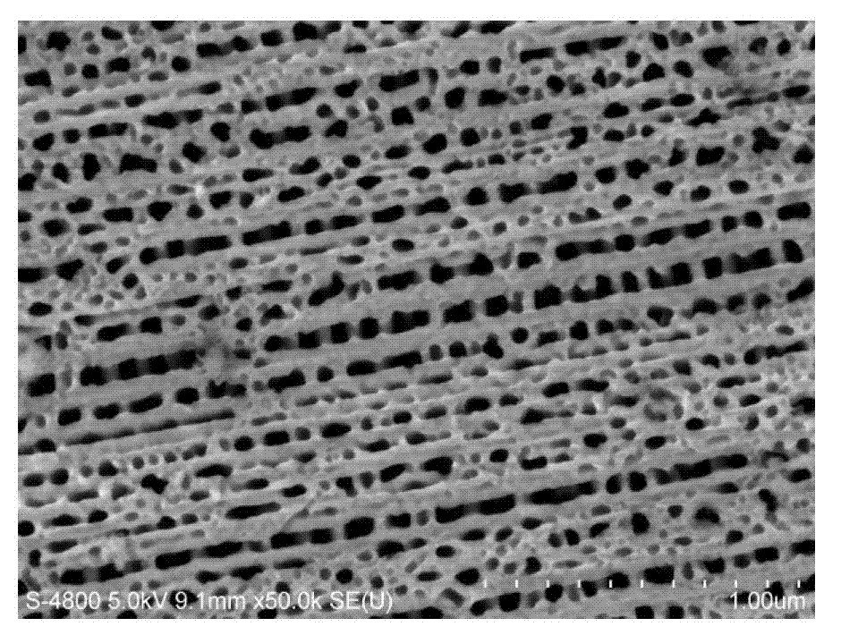
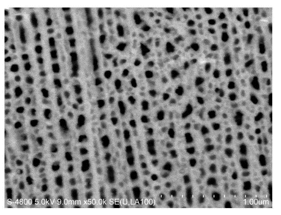
[0027] The process of constructing nano-trap on typical aluminum alloy substrate is as follows: figure 1 shown.

[0028] This patent proposes a method for effectively reducing the secondary electron emission coefficient on the surface of high-power microwave components. The core of this method is to use a series of treatment processes such as anodic oxidation, evaporative silver plating, and vacuum annealing on the basis of ensuring good electrical conductivity of microwave components to self-assemble nano-silver on the surface of the regular porous oxide film of aluminum alloy to form nano-trap. structure, in order to achieve the purpose of inhibiting SEY. The method mainly includes the following processing steps: After necessary cleaning, the microwave components are firstly coated with protective glue to protect the surface that does not need to be treated, and then electrochemically corroded by phosphoric acid to form a pore diameter of about 100nm on the surface of the a...


PUM

PropertyMeasurementUnit
thicknessaaaaaaaaaa
melting pointaaaaaaaaaa
pore sizeaaaaaaaaaa

Abstract

The invention relates to a method for inhibiting secondary electron emission of a microwave component surface by adopting a nanostructure plating layer. According to the method, a microwave component is subjected to necessary washing, and then is coated with a protection glue to protect the surface requiring no treatment; phosphoric acid is adopted to carry out an electrochemical etching treatment, such that a porous alumina film layer with a hole size of about 100 nm and a depth-to-width ratio more than 10 is formed on the surface of an aluminum alloy; repeated washing is performed to remove the protection glue; a layer of a silver layer with a thickness of about 50 nm is plated on the oxidation film through evaporation plating; and finally a vacuum heating treatment is performed. With the treatment of the method of the present invention, binding force of the plating layer and the substrate can be improved, and the characteristic of the significantly-reduced melting point of the nano-silver is adopted, such that the nano-silver is self-assembled on the surface of the oxidation layer to form a nano-trap structure while the continuity of the silver plating layer can be maintained well; and inhibition of secondary electron emission is achieved based on assurance of a certain electrical conductivity. The method of the present invention provides good cohesion for the existing microwave component treatment process, and the secondary electron emission coefficient of the microwave component surface is significantly inhibited.

Description

Technical field: [0001] The patent of the invention relates to the field of surface treatment of satellite microwave components, in particular to a method for suppressing secondary electron emission on the surface of microwave components by using a nanostructured coating. Background technique: [0002] At present, most of the microwave passive components in the satellite payload system are based on aluminum alloy. In order to reduce the loss of the device, the most commonly used method is the surface electrochemical silver plating. In actual use, these silver-plated parts are prone to multiplier discharge effect under the condition of high-power electromagnetic wave transmission, which is called micro-discharge phenomenon. Micro-discharge breakdown of microwave components is one of the main factors that determine the reliability and life of satellites. With the expansion of the operating range of microwave components, the need to suppress micro-discharge is becoming more an...

Claims


Application Information

Patent Timeline
Patent Type & Authority Applications(China)
IPC IPC(8): C25D11/04C23C14/16C23C14/58B82Y40/00
Inventor 张雯贺永宁胡少光康雪崔万照胡天存黄光孙
Owner XI AN JIAOTONG UNIV
Why Eureka
Try Eureka