Method for inhibiting secondary electron emission coefficient of dielectric material

A technology of secondary electron emission and dielectric materials, which is applied in the fields of material capacitance, analytical materials, and material resistance, and can solve problems such as complex process flow, poor applicability, and high cost of manpower and material resources

Pending Publication Date: 2021-07-06
XI AN JIAOTONG UNIV
View PDF3 Cites 0 Cited by
  • Summary
  • Abstract
  • Description
  • Claims
  • Application Information

AI Technical Summary

Problems solved by technology

The charging and discharging effect on the surface of the spacecraft will generate electromagnetic pulses with high voltage and high current, which will cause dysfunction of the internal components or components of the spacecraft, affect the communication and command transmission between the ground and the spacecraft in orbit, and cause serious damage to the spacecraft. Irreversible failure and obsolescence
Therefore, it is necessary to suppress the secondary electron emission coefficient on the surface of the dielectric material, and the traditional process of suppressing the secondary electron emission coefficient on the surface of the dielectric material is very complicated, poor in applicability, and relatively high in cost, requiring a lot of manpower and material resources

Method used


Image

  • Method for inhibiting secondary electron emission coefficient of dielectric material
  • Method for inhibiting secondary electron emission coefficient of dielectric material
  • Method for inhibiting secondary electron emission coefficient of dielectric material

Examples


Embodiment Construction

[0035] In order to make the purpose and technical solution of the present invention clearer and easier to understand. The present invention will be further described in detail below in conjunction with the drawings and embodiments. The specific embodiments described here are only used to explain the present invention, not to limit the present invention.

[0036] In the description of the present invention, it should be understood that the terms "installation", "connection" and "connection" should be understood in a broad sense, for example, it can be a fixed connection, a detachable connection, or an integral connection; it can be A mechanical connection can also be an electrical connection; it can be a direct connection or an indirect connection through an intermediary, and it can be the internal communication of two components. Those of ordinary skill in the art can understand the specific meanings of the above terms in the present invention in specific situations.

[0037]...


PUM


Abstract

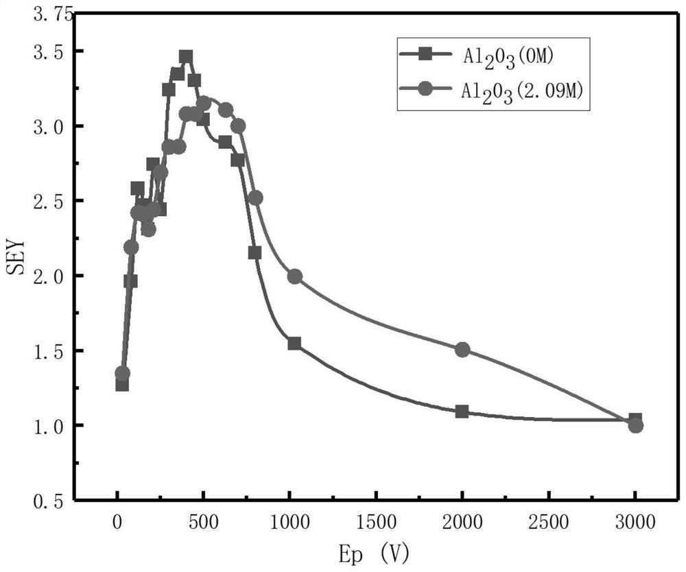
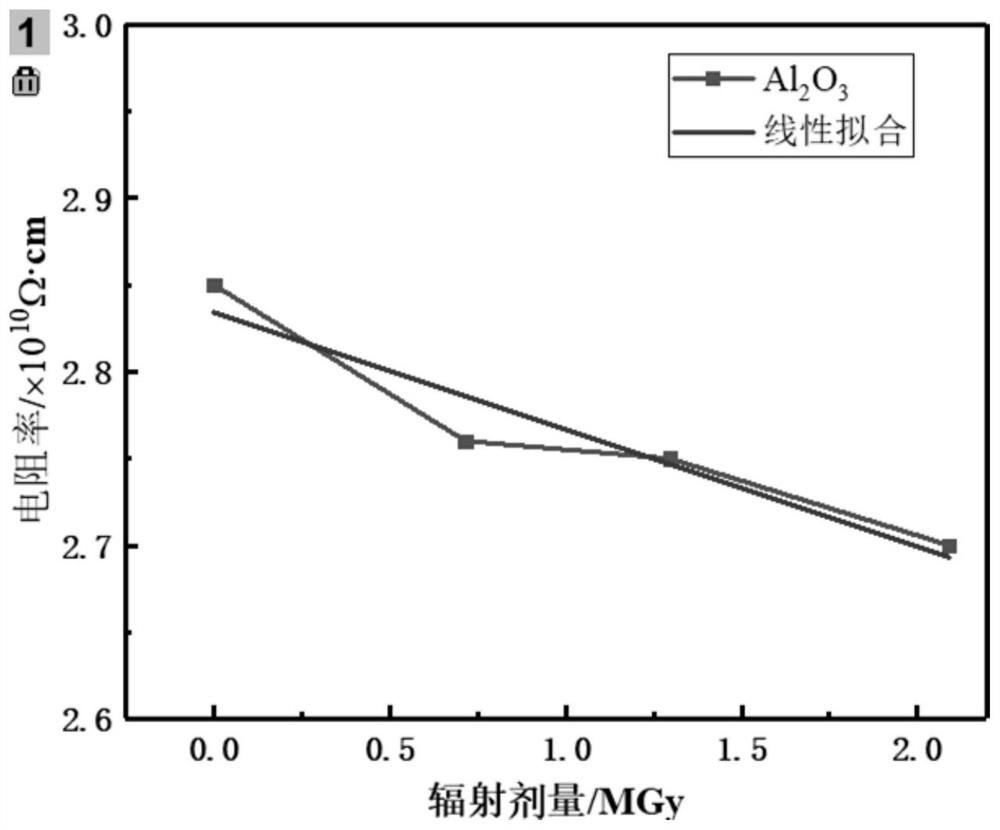
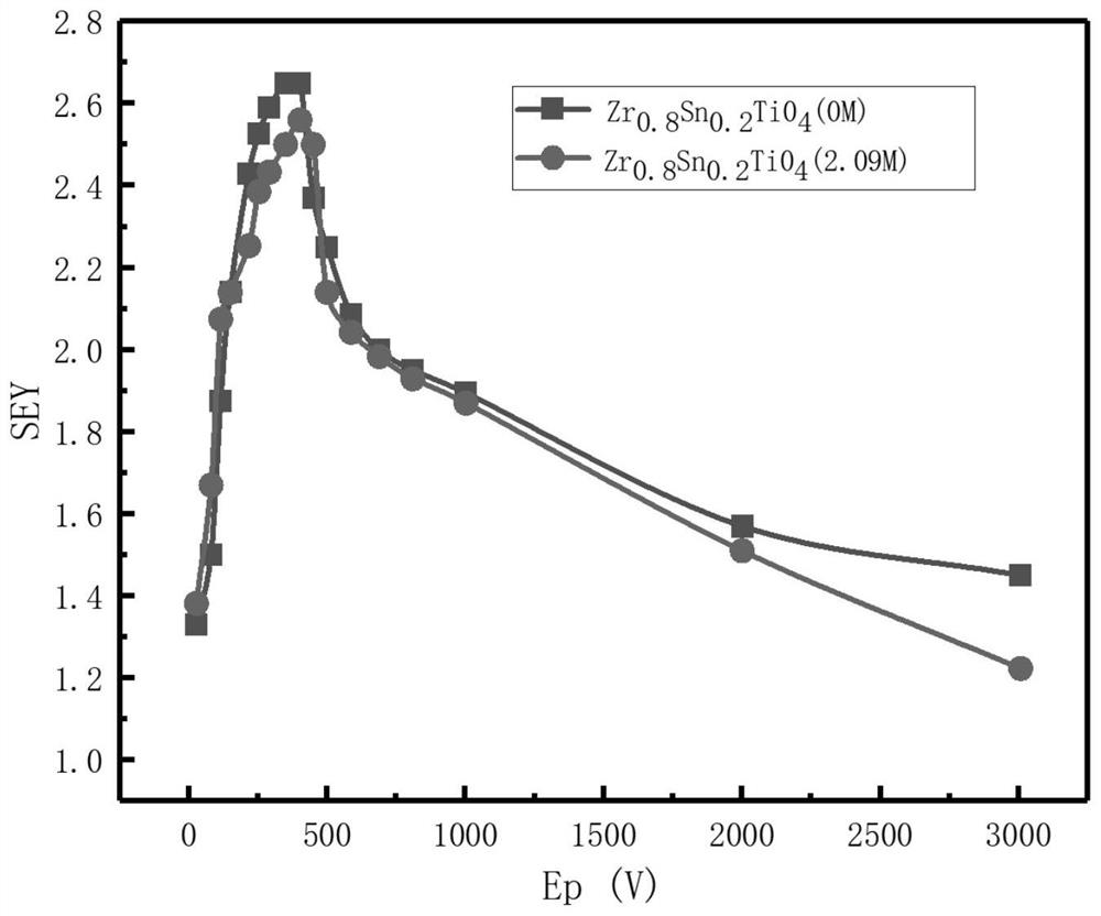
The invention discloses a method for inhibiting the secondary electron emission coefficient of a dielectric material, which comprises the following steps: selecting a ceramic sample and a polymer sample as research objects, and carrying out irradiation treatment on the samples by using gamma rays. Experiments prove that the resistivity of the dielectric material is reduced along with the increase of the irradiation dose, and the maximum value of the secondary electron emission coefficient is also reduced, so that the secondary electron emission coefficient of the dielectric material is inhibited to a certain extent. Compared with processes such as surface corrosion, photoetching and chemical methods for reducing the secondary electron emission coefficient, the method for inhibiting the secondary electron emission coefficient of a dielectric material through irradiation has the advantages of universality, simple process, low cost, simplicity and convenience in operation and the like.

Description

technical field [0001] The invention relates to the micro-discharge effect of a microwave device in a spacecraft, which is used for suppressing the secondary electron emission coefficient on the surface of a dielectric material. Background technique [0002] Discharge occurs when microwave devices operate at high frequency or high power, which is the microdischarge effect. Since the microdischarge phenomenon is often accompanied by the generation and emission of secondary electrons, it is also called the secondary electron multiplication effect. The micro-discharge effect is a special effect that will affect the payload of space spacecraft and the reliable operation on orbit. It will lead to the accumulation of charges on the surface of dielectric materials. When the charge accumulates to a certain extent, it will cause discharge and cause the failure of various components of the spacecraft, especially power devices. The impact of micro-discharge is very extensive. The sli...

Claims


Application Information

Patent Timeline
Patent Type & Authority Applications(China)
IPC IPC(8): C04B41/80C04B35/10C04B35/462C04B35/465C04B35/50G01N23/2202G01N23/2251G01N27/04G01N27/22
CPCC04B35/10C04B35/462C04B35/465C04B35/50C04B41/0045C04B41/80G01N23/2202G01N23/2251G01N27/04G01N27/221G01N2223/09
Inventor 向锋洪小飞顾腾刘潇帅董亦鹏
Owner XI AN JIAOTONG UNIV
Why Eureka
Try Eureka