Optical film manufacturing method, polarizing plate and image display device

A manufacturing method and optical film technology, which can be applied to devices, optics, and optical components that coat surfaces with liquids, can solve problems such as increased cost, insufficient effect, and limited width of optical films, and achieve high productivity.

Active Publication Date: 2012-10-17
SUMITOMO CHEM CO LTD
View PDF12 Cites 11 Cited by
  • Summary
  • Abstract
  • Description
  • Claims
  • Application Information

AI Technical Summary

Problems solved by technology

According to this method, it is considered that there is some effect on the above-mentioned problem of "residue of resin" remaining on the surface of the mold, but the effect on the problem of peeling and falling of the cured resin from the both end regions of the cured coating layer is not sufficient.
[0008] In addition, according to the method described in JP2007-203678

Method used


Image

  • Optical film manufacturing method, polarizing plate and image display device
  • Optical film manufacturing method, polarizing plate and image display device
  • Optical film manufacturing method, polarizing plate and image display device

Examples


Embodiment 1

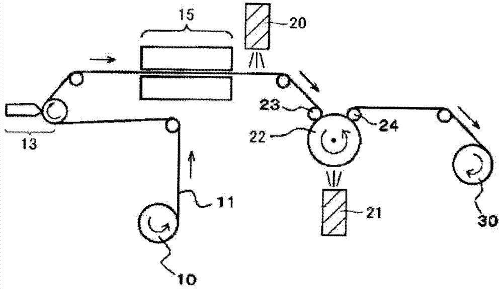
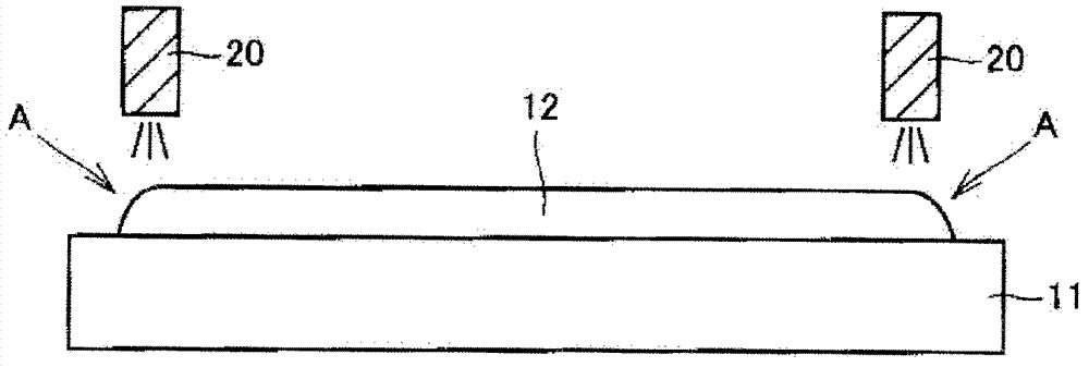
[0094] (1) Production of roll casting molds

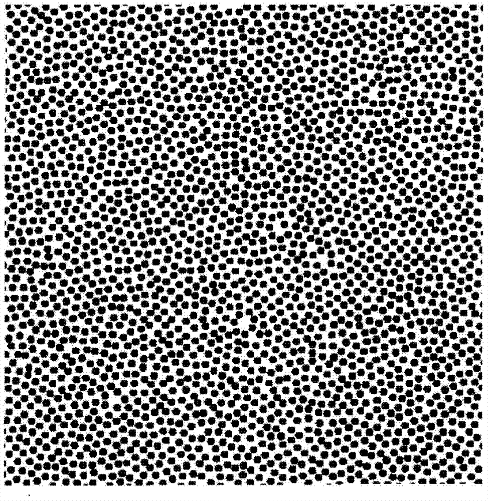
[0095] What performed ballard copper plating on the surface of the aluminum roll (A5056 based on JIS) of diameter 200mm was prepared. Ballard copper plating consists of copper plating / thin silver plating / surface copper plating, and the overall thickness of the plating is set to about 200 μm. The copper-plated surface was mirror-polished, and a photosensitive resin was applied to the polished copper-plated surface and dried to form a photosensitive resin film. Next, on the photosensitive resin film, use a laser to image 3 Expose and develop a pattern in which the pattern shown in is repeated. Exposure and development by laser were performed using Laser Stream FX (manufactured by Think Laboratory Co., Ltd.).

[0096] Again, as image 3 The image data of the pattern shown in is obtained by randomly arranging dots with a diameter of 16 μm, and was created with a size of 20.9 mm×20.9 mm and 12800 dpi. A positive photosensitive res...

Embodiment 2

[0106] Except that the cumulative light intensity in the UVA region of the first curing step is 30mJ / cm 2 Except for this, an optical film was produced in the same manner as in Example 1.

Embodiment 3

[0108] Except that the cumulative light intensity in the UVA region of the first curing step is 10mJ / cm 2 Except for this, an optical film was produced in the same manner as in Example 1.


PUM


Abstract

The optical film manufacturing method includes a coating procedure which coats a coating liquid containing the active energy ray curing resin on a substrate film to form a coated layer, a first curing procedure which irradiating the active energy ray to two end areas of the coated layer along the orthogonal direction of a transmission direction of the coated layer, a second curing procedure which irradiates the active energy ray to the coated layer from the substrate film under the condition that the surface of a casting model presses against the surface of the coated layer. According to the invention, the optical film manufacturing method can provide high quality and zero-defect optical film, and the production rate is high.

Description

technical field [0001] The present invention relates to a method for producing an optical film in which a coating solution containing an active energy ray-curable resin is coated on a base film and cured. In addition, the present invention relates to a polarizing plate and an image display device using the optical film. Background technique [0002] An optical film in which a resin layer having a predetermined optical function is formed by coating on a base film is used in various image displays such as liquid crystal display devices as an anti-glare film, a light diffusion film, a hard coat film, etc. device. [0003] Generally, the said resin layer which an optical film has is formed by apply|coating the coating liquid containing active energy ray-curable resin on a base film, and irradiating active energy ray to the obtained coating layer, and hardening it. In order to impart a desired shape to the surface of the coating layer depending on the optical properties require...

Claims


Application Information

Patent Timeline
IPC IPC(8): G02B1/10G02B5/30G02F1/1335B05D7/24B05D3/06B29C39/18B29C59/04B29L9/00B29L11/00G02B1/14
CPCB29C39/18B29C59/04B29D11/00644G02B1/10G02B5/3041
Inventor 神野亨神崎昌金玉馨金云基
Owner SUMITOMO CHEM CO LTD
Why Eureka
Try Eureka