crosswise double diffusion MOFET and manufacturing method thereof

A semiconductor and metal layer technology, applied in the field of lateral double-diffused metal-oxide-semiconductor field effect transistors, can solve the problems of high cost and complex manufacturing

Active Publication Date: 2012-10-17
CHENGDU MONOLITHIC POWER SYST
View PDF11 Cites 23 Cited by
  • Summary
  • Abstract
  • Description
  • Claims
  • Application Information

AI Technical Summary

Problems solved by technology

Therefore, the fabrication of conventional lateral DMOS 100 is not only complicated but also expensive

Method used


Image

  • crosswise double diffusion MOFET and manufacturing method thereof
  • crosswise double diffusion MOFET and manufacturing method thereof
  • crosswise double diffusion MOFET and manufacturing method thereof

Examples


Embodiment Construction

[0044] Some embodiments of the present invention will be described in detail below. In the following description, some specific details, such as specific circuit structures in the embodiments and specific parameters of these circuit elements, are used to provide a better understanding of the embodiments of the present invention. It will be understood by those skilled in the art that embodiments of the invention may be practiced even without some details or other combinations of methods, elements, materials, and the like.

[0045] In the description and claims of the present invention, if words such as "left, right, inside, outside, front, back, up, down, top, above, bottom, under" etc. are used, they are only For ease of description, no inevitable or permanent relative positions of components / structures are shown. It should be understood by those skilled in the art that such terms are interchangeable under appropriate circumstances, for example, so that the embodiments of the...


PUM


Abstract

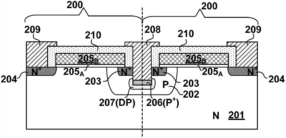
The invention provides a crosswise DMOS with cupped source electrode contact and a method for forming the crosswise DMOS. The crosswise DMOS comprises a cupped source electrode contact, wherein the cupped source electrode contact comprises a cupped part which longitudinally extends and penetrates the source area of the crosswise DMOS and contacts the body area,and the cupped part is electrically coupled with the source area and the body area. The crosswise DMOS not only has smaller size, but also is low in production cost.

Description

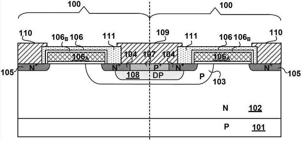
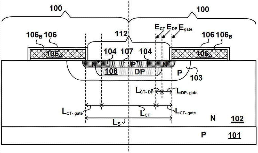
[0001] Related references [0002] This application claims priority to and benefit from, and is hereby incorporated in its entirety by, Patent Application No. 13 / 213,011 filed in the United States on August 18, 2011. technical field [0003] Embodiments of the present invention relate to semiconductor devices, and more particularly, to lateral double-diffused metal-oxide-semiconductor field effect transistors. Background technique [0004] Lateral double-diffused metal-oxide-semiconductor field-effect transistors (LDMOS) are widely used in various integrated power management circuits. Generally, LDMOS is used as a power transistor in these power management circuits to continuously switch on and off in response to a control signal to realize power conversion. [0005] Figure 1A A schematic longitudinal cross-sectional view of an LDMOS 100 is shown. Such as Figure 1A As shown, the LDMOS 100 can be formed on a P-type semiconductor substrate 101 . The LDMOS 100 may include ...

Claims


Application Information

Patent Timeline
Patent Type & Authority Applications(China)
IPC IPC(8): H01L29/06H01L29/36H01L21/336
CPCH01L29/66689H01L29/0878H01L29/456H01L29/086H01L29/1095H01L29/7816H01L29/66696H01L29/42368H01L29/4933H01L29/665H01L29/41766
Inventor 唐纳徳·迪斯尼
Owner CHENGDU MONOLITHIC POWER SYST
Why Eureka
Try Eureka