Chip cutting method for increasing LED chip light extraction

A technology of LED chips and cutting methods, applied in laser welding equipment, fine working devices, stone processing equipment, etc., can solve problems such as full inspection of chips, not much help in brightness, abnormal packaging electrical parameters, etc.

Active Publication Date: 2012-10-17
JIANGSU ETERN +1
View PDF10 Cites 6 Cited by
  • Summary
  • Abstract
  • Description
  • Claims
  • Application Information

AI Technical Summary

Problems solved by technology

At present, most LED chips are split into individual grains after saw blade or back scribing. This kind of chip cracking process is just a simple physical splitting process of grains, which does not help much to improve brightness. Prone to appearance problems such as parallelogram and chipping
In order to overcome this problem, in the actual production, GaN-based blue-green chips are used for front-scribing and back-cracking to reduce the generation of defective chips. Absorbs a large amount of light, reducing the brightness of the chip by about 20%
In order to remove the ablation caused by laser scribing, the wet etching method is currently used to remove the scribing ablation and improve the light extraction efficiency, but this method can easily lead to full inspection of the chip, abnormal packaging electrical parameters (voltage increase, etc.), and operation It is complex and requires timely preparation, replacement of acid (alkali) solution for corrosion, heating, etc., and there are great safety hazards at the same time
It is also reported that dry etching is used. The disadvantage is that the powder ablated by laser is easy to splash out during the etching process, and remains on the surface of the chip to form a protective layer, which seriously affects the etching rate, and the scattered powder is random. It is difficult to completely unify the etching depth
The disadvantage of this patent document is that before scribing, it is necessary to remove the epitaxial silicon layer in the pre-drawn groove area on the front side of the semiconductor optoelectronic component chip, and then use laser to draw a guide groove on the surface of the substrate from which the epitaxial silicon layer has been removed. Groove; the chip has not been divided into crystal grains before cutting with a diamond knife, so it is impossible to accurately grasp the depth of the laser marking. In order to meet the requirements of removing all the black ablation drawn by the laser, it is necessary to cut off as many laser scratches as possible Substances nearby can easily cause diamond knife wear and form lateral and radial cracks on both sides of the groove

Method used


Image

  • Chip cutting method for increasing LED chip light extraction
  • Chip cutting method for increasing LED chip light extraction
  • Chip cutting method for increasing LED chip light extraction

Examples


Embodiment Construction

[0008] Technical scheme of the present invention is as follows:

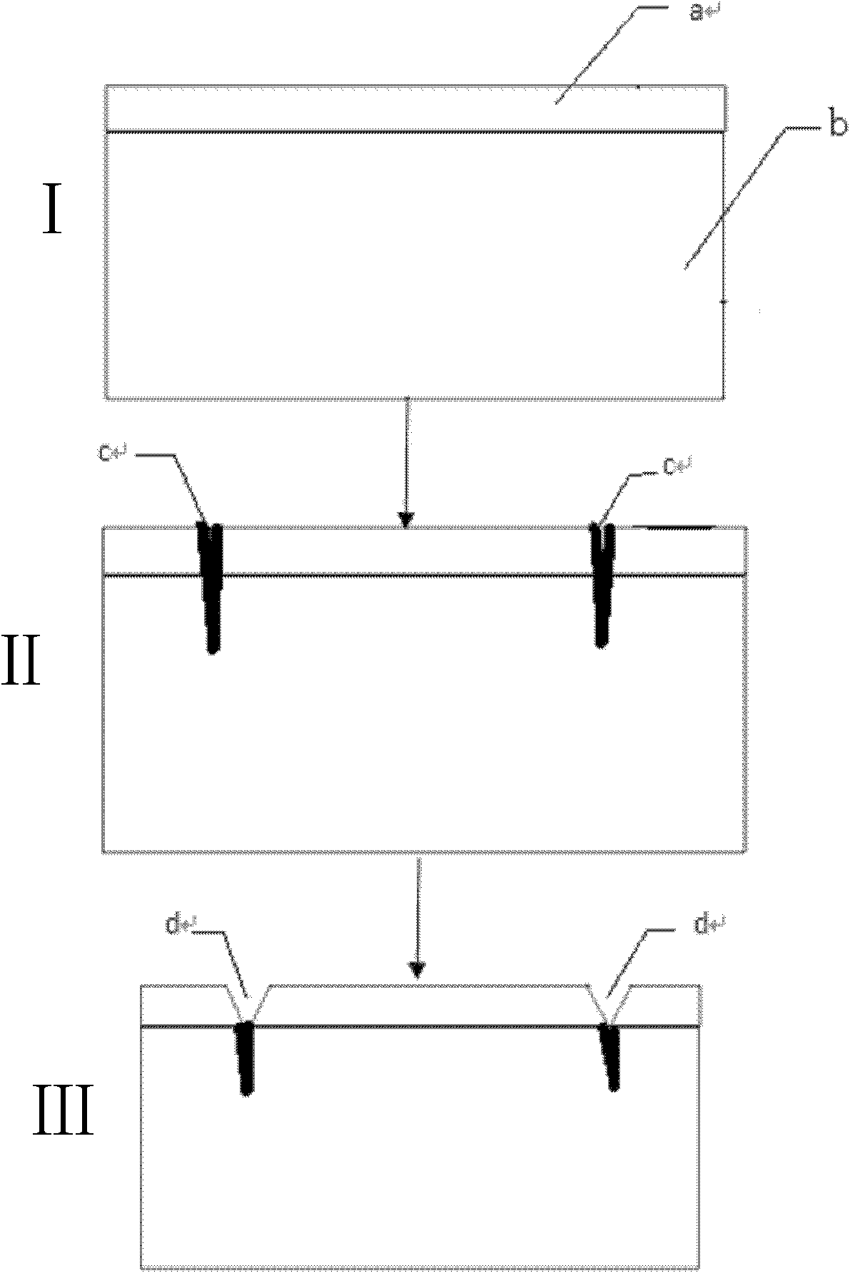
[0009] A chip cutting method for improving light output of LED chips, comprising the steps of:

[0010] (1) Chip preparation: the chip is an epitaxial wafer with an epitaxial layer grown on a substrate, and the upper surface of the epitaxial layer is the front side of the chip.

[0011] (2) Laser scribing: use a laser to draw scratches with a depth of 30±5 μm and a width of 6±2 μm.

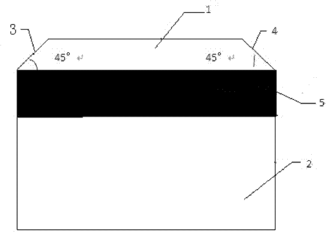
[0012] (3) Saw blade: Use a diamond saw blade to cut along the saw blade. The saw blade is a left-right symmetrical isosceles inverted triangle. Form a tapered opening with an inclination angle of 30° to 60°; adjust the height of the saw blade so that the epitaxial layer is just sawed through; the width of the saw blade is 20±4 μm.

[0013] (4) Splinter: Flip the sawed chip over and pour the film, and use a split knife to scratch the chip along the above-mentioned laser on the back of the chip to form crystal grains.

[0014] The...


PUM

PropertyMeasurementUnit
thicknessaaaaaaaaaa

Abstract

A chip cutting method for increasing LED chip light extraction is disclosed. The method comprises the following steps: using a laser to make a scratch on a right side of the chip; then, using a diamond saw blade knife to carry out saw blade along the scratch, wherein the saw blade knife is a bilaterally symmetrical isosceles inverted triangle and an included angle of a knife side surface and a horizontal line is 30-60 DEG; adjusting a knife height of the saw blade knife so that an epitaxial layer is just sawed through; carrying out overturn and inverted membrane on the chip after the saw blade is finished; using a splinter knife to carry out splinter on a back side of the chip along the laser scratch. According to the invention, through a saw blade technology, an epitaxial layer edge of the chip, which is about 10micron, is sawed into an inclined platform. A chip light extraction rate can be increased by more than 20%. Simultaneously, chip appearance is improved. A technology operation is simple and is easy to be realized.

Description

technical field [0001] The invention relates to a light-emitting diode (LED) chip cutting process, in particular to a cutting method for improving the light output of the LED chip, and belongs to the technical field of semiconductor chips. Background technique [0002] Scribing and splitting in the LED chip manufacturing process is to divide the whole chip into a single grain of the required size, which is an essential process in the semiconductor light-emitting diode chip manufacturing process. At present, most LED chips are split into grains by saw blade or back scribing. This kind of chip cracking process is just a simple physical splitting process of grains, which does not help much to improve brightness. It is prone to appearance problems such as parallelogram and edge collapse. In order to overcome this problem, in the actual production, GaN-based blue-green chips are used for front-scribing and back-cracking to reduce the generation of chip cutting defects, but the b...

Claims


Application Information

Patent Timeline
Patent Type & Authority Applications(China)
IPC IPC(8): H01L33/00B28D5/00B23K26/00
Inventor 黄少梅沈燕李树强王成新刘青
Owner JIANGSU ETERN
Why Eureka
Try Eureka