Chip cutting method for increasing LED chip light extraction
A technology of LED chips and cutting methods, applied in laser welding equipment, fine work equipment, stone processing equipment, etc., can solve the problems of parallelogram, not much help in brightness, abnormal packaging electrical parameters, etc.
- Summary
- Abstract
- Description
- Claims
- Application Information
AI Technical Summary
Problems solved by technology
Method used
Image
Examples
Embodiment Construction
[0008] Technical scheme of the present invention is as follows:
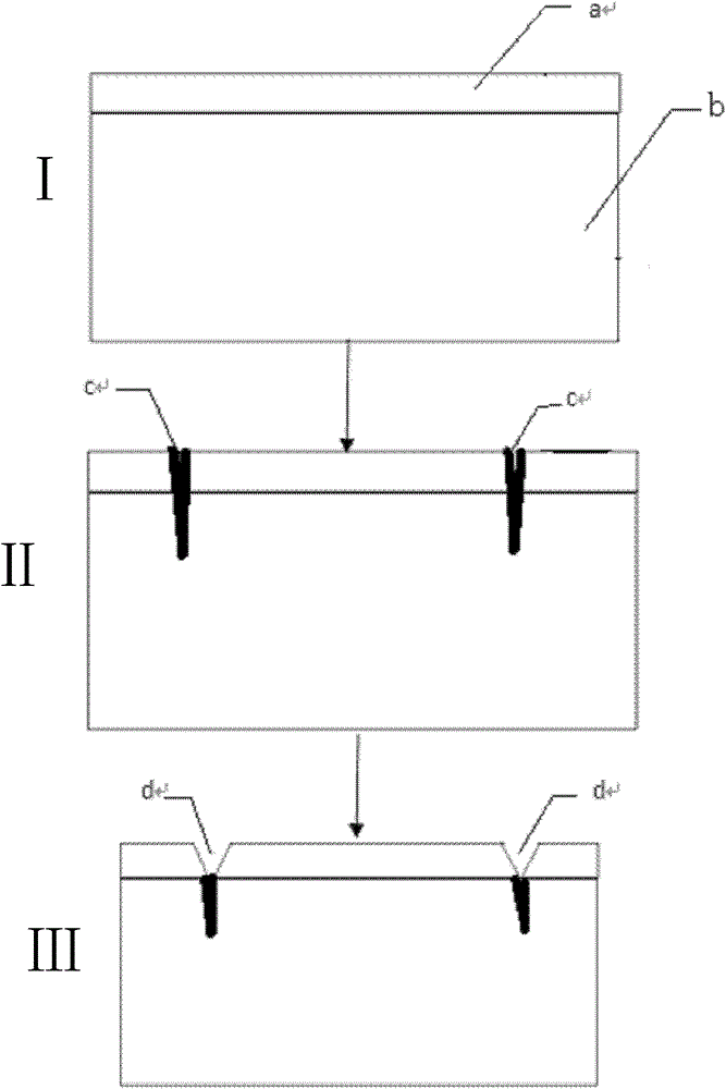
[0009] A chip cutting method for improving light output of LED chips, comprising the steps of:
[0010] (1) Chip preparation: the chip is an epitaxial wafer with an epitaxial layer grown on a substrate, and the upper surface of the epitaxial layer is the front side of the chip.
[0011] (2) Laser scribing: use a laser to draw scratches with a depth of 30±5 μm and a width of 6±2 μm.
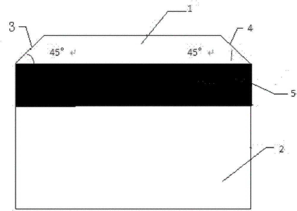
[0012] (3) Saw blade: Use a diamond saw blade to cut along the saw blade. The saw blade is a left-right symmetrical isosceles inverted triangle. Form a tapered opening with an inclination angle of 30° to 60°; adjust the height of the saw blade so that the epitaxial layer is just sawed through; the width of the saw blade is 20±4 μm.
[0013] (4) Splinter: Flip the sawed chip over and pour the film, and use a split knife to scratch the chip along the above-mentioned laser on the back of the chip to form crystal grains.
[0014] The...
PUM
| Property | Measurement | Unit |
|---|---|---|
| thickness | aaaaa | aaaaa |
Abstract
Description
Claims
Application Information


