
Eureka
For R&D, Eureka makes reading and utilizing patents & technical documents easy.
Eureka AIR
Designed for self-driven R&D workflows. Generate viable solutions, solve complex R&D challenges, empower your innovation with AI.

Eureka Materials
Designed for material experts only. Revolutionize your material R&D, from search, analyze, to developing new materials.

TechResearch
Generate reliable direction feasibility study reports for your R&D in just a few steps.

TechSeek
Discover and master advanced knowledge NOW. Basics, ideas, possibilities, all at once.

TechMind
As an expert in R&D Theories, TechMind can generates customized viable solutions instantly.

TechRisk
Analyze your overall solution with one click, know your potential R&D risks in advance.

TechMonitor
Get weekly tech updates, stay abreast of the latest tech innovations and key insights.
Source or emitter follower buffer circuit and method
A buffer circuit, emitter follower technology, used in amplifiers with impedance circuits, electrical components, amplifiers with semiconductor devices/discharge tubes, etc.
- Summary
- Abstract
- Description
- Claims
- Application Information
AI Technical Summary
Problems solved by technology
Method used
Image

Examples
Embodiment Construction
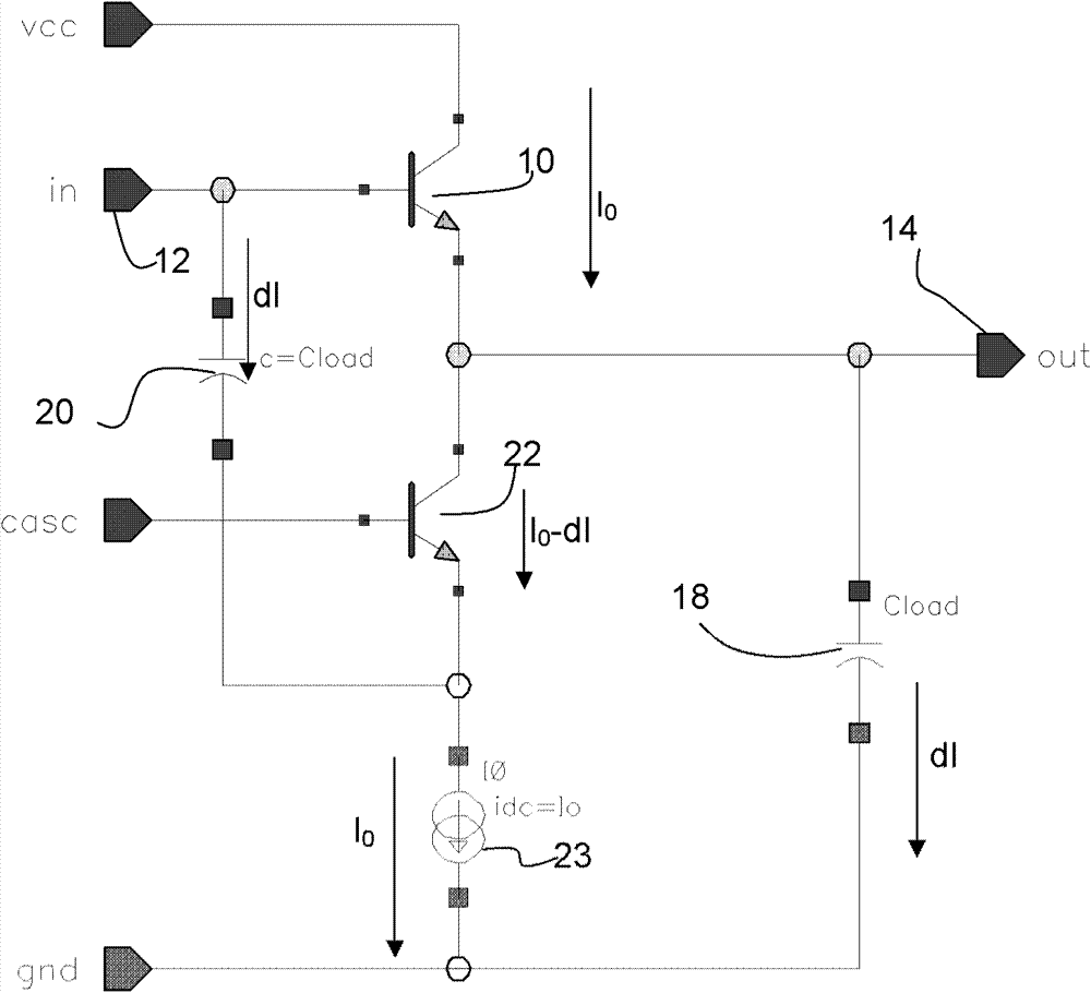
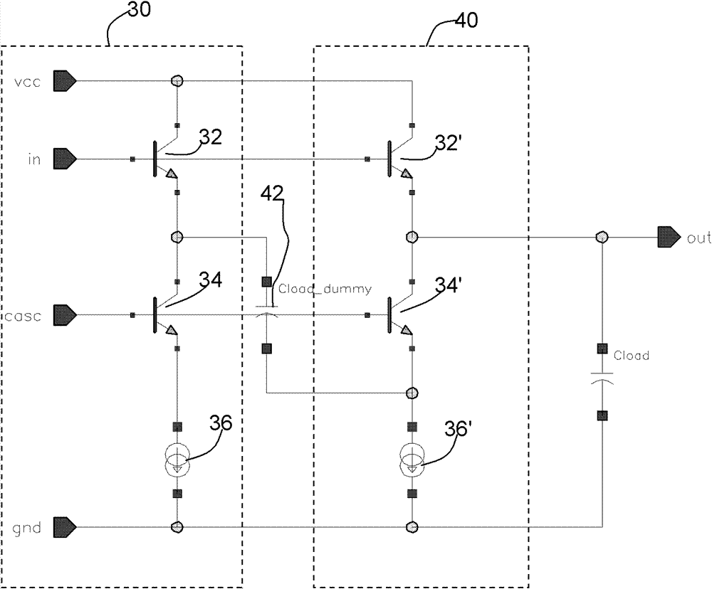
[0045] In one aspect, the invention proposes a buffer circuit comprising a source or emitter follower input stage and an output stage. A load is placed between the stages, the load comprising a reproduction of the output load of the buffer circuit. This improves the linearity of the circuit while enabling high input impedance. In another aspect, the buffer circuit includes a source or emitter follower output stage. The loading is in the form of a filter and includes a reproduction of the output loading of the buffer circuit. This enables compensation of current through more complex output loads, improving linearity for a wide range of applications.
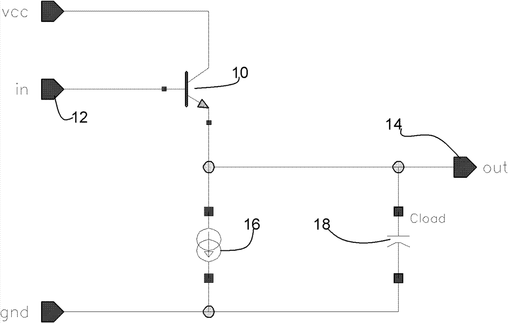
[0046] figure 1 A basic source / emitter follower circuit is shown.
[0047] Transistor 10 is a BJT in the case of an emitter follower and a FET in the case of a source follower. The circuit input 12 is applied to the base / gate and the collector / drain is connected to the high voltage rail VCC. The emitter / source is coupled to ...
PUM
 Abstract
Description
Claims
Application Information
 - R&D Engineer
- R&D Manager
- IP Professional
- Industry Leading Data Capabilities
- Powerful AI technology
- Patent DNA Extraction
Browse by: Latest US Patents, China's latest patents, Technical Efficacy Thesaurus, Application Domain, Technology Topic, Popular Technical Reports.
© 2024 PatSnap. All rights reserved.Legal|Privacy policy|Modern Slavery Act Transparency Statement|Sitemap|About US| Contact US: help@patsnap.com