Voltage mode transceiver having programmable voltage swing and external reference-based calibration

a voltage mode transceiver and voltage mode technology, applied in logic circuit coupling/interface arrangement, pulse technique, baseband system details, etc., can solve the problems of substantial variations, voltage mode driver circuits that require accurate voltage references, and substantially higher power consumption in current mode drivers than voltage mode drivers. achieve the effect of low input capacitan

Active Publication Date: 2006-11-14
MEDIATEK INC
View PDF2 Cites 63 Cited by
  • Summary
  • Abstract
  • Description
  • Claims
  • Application Information

AI Technical Summary

Benefits of technology

[0019]Use of the calibrated resistor network circuits enables the voltage mode transmit driver to create a constant output impedance driver that precisely matches the transmission line impedance, enabling the peak to peak differential voltage swing between the first and second differential signals to be programmed between a supply voltage (e.g., VDD) and a base voltage (e.g., ground).
[0020]In addition, the use of pull-up circuits and pull-down circuits sharing gate signals enables the input termination module to achieve a substantially low input capacitance. Moreover, the addition of an on-chip common-mode capacitive coupling to ground provides high frequency common mode termination without consumption of additional DC power.
[0021]Use of replicas in the calibration circuit enables the calibration circuit to periodically correct for variations in the integrated circuit due to noise, as well as systemic offsets that affect calibration values, ensuring that the binary code and the input calibration value at optimal levels.

Problems solved by technology

Hence, power consumption is substantially higher in a current mode driver circuit than a voltage mode driver circuit.
Hence, one disadvantage is that the voltage mode driver circuit requires accurate voltage references.
However, a problem in implementing a voltage mode driver circuit is that substantial variations in process or manufacturing techniques, voltage supply, and operating temperatures may cause substantial variations in the silicon structure which that implements the digital driver circuitry that includes the voltage mode driver.
Hence, process variations during fabrication and temperature variations can change input / output impedances by a sufficient degree that static impedance matching techniques are insufficient.

Method used


Image

  • Voltage mode transceiver having programmable voltage swing and external reference-based calibration
  • Voltage mode transceiver having programmable voltage swing and external reference-based calibration
  • Voltage mode transceiver having programmable voltage swing and external reference-based calibration

Examples


Embodiment Construction

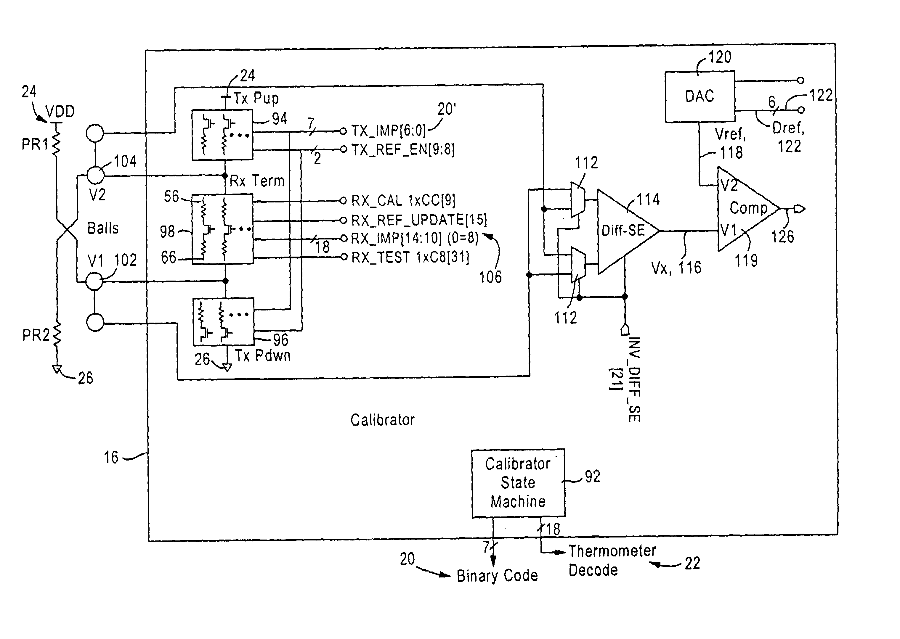
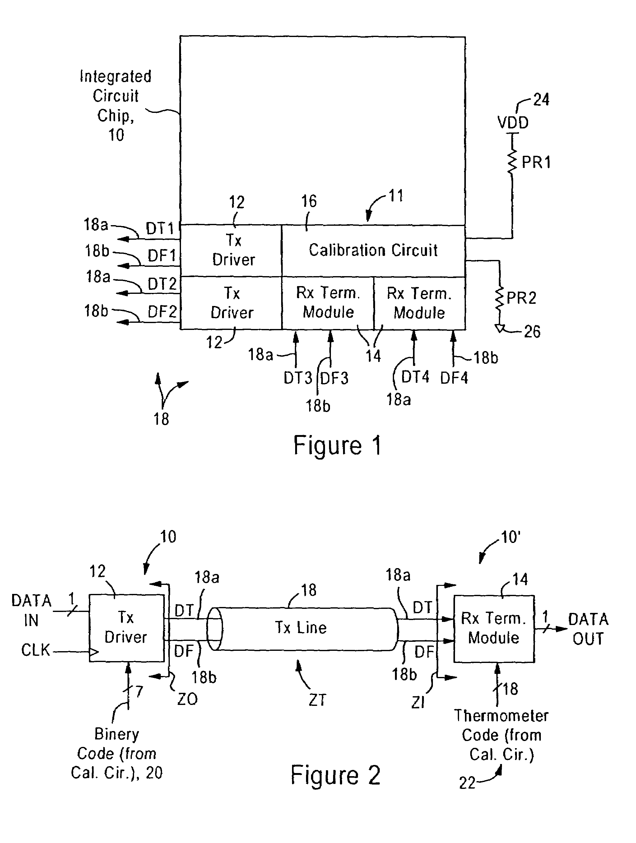
[0034]The disclosed embodiment is directed to an integrated circuit, for example a microprocessor or a device that interfaces with the microprocessor via a high-speed link such as a HyperTransport™ link, having a voltage mode transmit driver, an input termination module, and a calibration module. The voltage mode transmit driver is configured for setting an output impedance for a transmission line. The input termination module is configured for setting an input impedance for a transmission line, and the calibration module is configured for providing control signals to the voltage mode transmit driver and the input termination network.

[0035]FIG. 1 is a diagram illustrating an integrated circuit chip 10 having a plurality of voltage mode transmit drivers 12, input termination modules 14, and at least one calibration circuit 16, according to an embodiment of the present invention. The voltage mode transmit drivers 12 are configured for outputting differential signals “data true” (DT) a...


PUM


Abstract

An integrated device includes a voltage mode transmit driver for matching an output impedance to an output transmission line based on a binary code, an input termination module configured for matching an input impedance to an input transmission line based on an input impedance calibration value using thermometer-based decoding. The voltage mode transmit driver includes, for each differential output signal, a resistor network circuit having pull-up circuits and pull-down circuits for changing the voltage on the differential output signal, and having binary weighted resistance values relative to each other. The input termination module includes pull-up circuits and pull-down circuits having inverse hyperbolic resistance values relative to each other, and using thermometer-based decoding to ensure a linear change in input impedance during transitions in the input impedance calibration value. A calibration circuit generates the binary code and the input impedance calibration value based on replicas of the pull-up and pull-down circuits.

Description

BACKGROUND OF THE INVENTION[0001]1. Field of the Invention[0002]The present invention relates to driver circuits in digital systems for adjusting input impedance and output impedance of respective receivers and transmitters relative to a prescribed impedance of a transmission line.[0003]2. Background Art[0004]Newer processor architecture designs require transfer of data between large integrated circuits at higher speeds. These higher speeds require that the integrated circuits have input / output impedances that precisely match the prescribed impedance of the PC board traces interconnecting the integrated circuits. In particular, impedance matching is needed to minimize signal reflections caused by a change in impedance at the interface between a signal trace on the PC board and an integrated circuit chip. For example, HyperTransport™ technology specifies a data rate of 1.6 Gbps between each wire pair based on a double data rate using an 800 MHz clock. Hence, precise impedance matchin...

Claims


Application Information

Patent Timeline
Patent Type & Authority Patents(United States)
IPC IPC(8): H03K17/16
CPCH03K17/164H03K19/0005H04L25/0278H04L25/028
Inventor TALBOT, GERALD ROBERTSCHEFFER, MATTHEWHYPHER, AUSTEN JOHN
Owner MEDIATEK INC
Why Eureka
Try Eureka