Optical module for optical network unit

A technology of optical modules and detection modules, which is applied in the direction of electrical components, electromagnetic wave transmission systems, transmission systems, etc., can solve the problems of no-light LOS/SD instability, optical detection signal output errors, etc., and reduce the output error of optical detection signals probability, improve accuracy, and avoid output errors

Active Publication Date: 2012-10-24
HISENSE BROADBAND MULTIMEDIA TECH
2 Cites 11 Cited by

AI-Extracted Technical Summary

Problems solved by technology

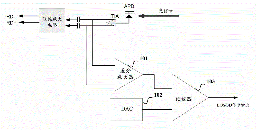
[0009] In addition, when the noise amplitude of the power supply and ground on the BOX board exceeds 50mV, the noise can pass through the power supply and be introduced by the module TIA, resulti...

Abstract

The invention discloses an optical module for an optical network unit, comprising a response current detection module and an MCU (micro-program control unit). The current input end of the response current detection module is connected with the cathode of a photodiode in the optical module. The response current detection module is used for detecting the response current outputted by the photodiode and outputting the corresponding voltage from the voltage output end thereof according to the response current. The voltage input end of the MCU is connected with the voltage output end of the response current detection module. The MCU is used for detecting the voltage outputted by the response current detection module, judging whether to receive the effective optical signal or not and controlling the output of the optical detection signal according to the judgment result. The receiving of the effective optical signal is judged according to the response current generated by the photodiode, and the response current generated by the photodiode is not easy to be affected by power supply and other interference sources, so that the optical detection signal output accuracy is improved greatly.

Application Domain

Electromagnetic transmission

Technology Topic

EngineeringPower flow +7

Image

  • Optical module for optical network unit
  • Optical module for optical network unit
  • Optical module for optical network unit

Examples

  • Experimental program(1)

Example Embodiment

[0039] In order to make the object, technical solution and advantages of the present invention clearer, the present invention will be described in further detail below with reference to the accompanying drawings and preferred embodiments. However, it should be noted that many of the details listed in the specification are only for readers to have a thorough understanding of one or more aspects of the present invention, and these aspects of the present invention can be implemented even without these specific details.
[0040] As used herein, terms such as "module" and "system" are intended to include computer-related entities such as, but not limited to, hardware, firmware, a combination of hardware and software, software, or software in execution. For example, a module may be, but is not limited to being limited to being, a process running on a processor, a processor, an object, an executable, a thread of execution, a program, and/or a computer.
[0041] The main idea of ​​the present invention is that the photodiode in the ONU optical module will generate a corresponding response current Ipd after detecting the optical signal; by monitoring the Ipd to judge whether an effective optical signal is received, thereby outputting a corresponding optical detection signal. Since the response current Ipd generated by the photodiode is hardly affected by the power supply or other interference sources, it is judged based on Ipd whether an effective optical signal is received, and the corresponding optical detection signal is output, which greatly avoids the phenomenon of wrong output of the optical detection signal , improving the accuracy of the light detection signal output.
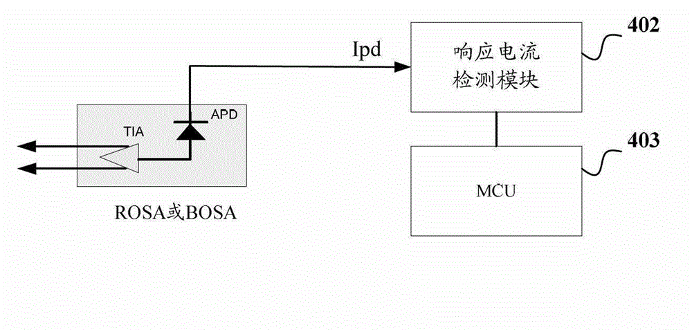
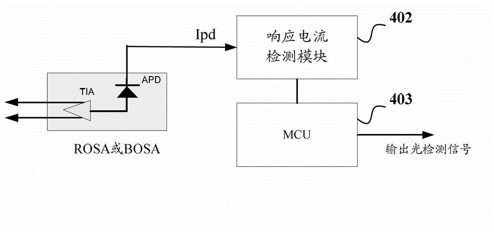
[0042] The technical solutions of the embodiments of the present invention will be described in detail below in conjunction with the accompanying drawings. The ONU optical module of the embodiment of the present invention, such as Figure 2a As shown, it includes: ROSA or BOSA, a response current detection module 402 , and an MCU (Microprogrammed Control Unit, microprogrammed control unit) 403 .
[0043] ROSA or BOSA includes a photodiode and a TIA; after the photodiode detects an optical signal, it outputs a corresponding response current Ipd; generally speaking, the stronger the power of the optical signal detected by the photodiode, the greater the output Ipd. The photodiode can specifically be an APD (Avalanche Photo Diode, avalanche photodiode) applied to an ONU optical module of a GPON network, or a PIN photodiode (in P, N junctions) applied to an ONU optical module of an EPON network. An I region close to the intrinsic material is added between them to form a semiconductor photodetector with a PIN structure).
[0044] The cathode of the photodiode is connected to the current input terminal of the response current detection module 402 , and the Ipd output by the photodiode flows into the response current detection module 402 . The response current detection module 402 is used to detect Ipd, and output a corresponding voltage from its voltage output terminal according to the input Ipd. That is to say, the output voltage of the response current detection module 402 changes with the change of the input Ipd, specifically, the two may have a proportional relationship. In other words, the output voltage of the response current detection module 402 can reflect the input Ipd, and further can reflect the power of the optical signal detected by the photodiode.
[0045] A voltage input terminal of the MCU 403 is connected to the voltage output terminal of the response current detection module 402 to detect the voltage output by the response current detection module 402 . The MCU 403 judges whether an effective light signal is received according to the detected voltage output by the response current detection module 402 ; and the MCU 403 controls the output of the light detection signal according to the judgment result.
[0046] like image 3 As shown, the above-mentioned current detection module 402 specifically includes: a current mirror circuit 501 and a sampling resistor 502 .
[0047] The current input terminal of the current mirror circuit 501 is connected to the cathode of the photodiode to receive the Ipd output by the photodiode. The Ipd output by the photodiode flows into the current mirror circuit 501; the mirror current output terminal of the current mirror circuit 501 is connected to the sampling resistor 502, and the mirror current of Ipd flows into the power supply ground through the sampling resistor 502, that is, the mirror current output terminal of the current mirror circuit 501 passes the sampling Resistor 502 is connected to power ground.
[0048] The connection point between the mirror current output terminal of the current mirror circuit 501 and the sampling resistor 502 serves as the voltage output terminal of the response current detection module 402 , so the voltage on the sampling resistor 502 is the output voltage of the current detection module 402 . MCU403 detects the output voltage of the current detection module 402, that is, detects the voltage on the sampling resistor 502, and the voltage on the sampling resistor 502 reflects the size of the mirror current of the current mirror circuit 501, and the mirror current of the current mirror circuit 501 reflects the flow-in Ipd The size of , also reflects the power of the optical signal detected by the photodiode.
[0049] MCU403 according to the detected voltage output by the response current detection module 402, the method for judging whether to receive an effective optical signal can be: if the MCU403 determines that the detected voltage is greater than the first threshold value set, then judge that an effective optical signal is received; If the MCU 403 determines that the detected voltage is lower than the set second threshold, it determines that no effective optical signal is received. Those skilled in the art may set the first threshold and the second threshold according to actual conditions, and the set first threshold and the second threshold may be equal or unequal. If the first threshold is not equal to the second threshold, a hysteresis interval is between the first threshold and the second threshold. For example, if the first threshold is 200 and the second threshold is 100, then MCU403 determines that when the detected voltage is greater than 200, it determines that an effective optical signal is received; when MCU403 determines that the detected voltage is less than 100, it determines that no effective optical signal is received; Between 100 and 200 is the hysteresis interval.
[0050] One of the easiest implementation methods for MCU403 to control the output of light detection signals is as follows: Figure 2b As shown, MCU403 uses one of its output ports as the output port of the light detection signal. For example, for the situation that MCU403 uses one of its output ports as the SD signal output port: if MCU403 judges to receive an effective optical signal, then output a high level from the output port; if MCU403 judges that no effective optical signal is received, then This output port outputs low level.
[0051] Or, for the situation that MCU403 uses one of its output ports as the LOS signal output port: if MCU403 judges to receive an effective optical signal, then output a low level from the output port, if MCU403 judges that no effective optical signal is received, then from This output port outputs high level.
[0052] Further, the ONU optical module further includes: an optical detection signal output circuit 404 .
[0053] A simple implementation method of the light detection signal output circuit 404 is as follows: Figure 2c As shown, the light detection signal output circuit 404 is an inverter, and the input end of the inverter is connected to the light detection signal control output end of the MCU 403 . For the case where the optical detection signal is an SD signal: if the MCU403 judges that a valid optical signal is received, it will output a low level from its optical detection signal control output, and the inverter will output a high level; If the optical signal is detected, the control output terminal of the optical detection signal outputs a high level, and the inverter outputs a low level.
[0054] For the case where the light detection signal is a LOS signal: if MCU403 judges that a valid light signal is received, it will output a high level from its light detection signal control output terminal, and the inverter will output a low level; If the optical signal is detected, the control output terminal of the light detection signal outputs a low level, and the inverter outputs a high level.
[0055] Another specific circuit of the light detection signal output circuit 404 is as Figure 4 As shown, it includes: a differential amplifier 601 , a DAC (Digital-to-Analog Converter, digital-to-analog converter) 602 , a comparator 603 , and a logic operator 604 .
[0056] The differential signal input terminal of the differential amplifier 601 is connected to the differential signal output terminal of the TIA, and the differential signal output by the TIA is input into the differential amplifier 601; or, the differential signal input terminal of the differential amplifier 601 is connected to the differential signal output terminal of the TIA through a capacitor, The differential signal output by the TIA is coupled to the differential amplifier 601 through a capacitor. The differential amplifier 601 outputs a corresponding voltage from the voltage output terminal according to the amplitude difference of the input differential signal.
[0057] The input terminal of DAC602 is connected with MCU403 to receive the data written by MCU403, store the received data in the register, and output corresponding voltage from its output terminal according to the received data.
[0058] One voltage input terminal of the comparator 603 is connected with the voltage output terminal of the differential amplifier 601 ; the other voltage input terminal of the comparator 603 is connected with the output terminal of the DAC602 .
[0059] An input terminal of the logical operator 604 is connected with the output terminal of the comparator 603, and another input terminal of the logical operator 604 is connected with a control output terminal of the MCU403; the signal output by the output terminal of the logical operator 604 is the light detection signal , that is, the output terminal of the logic operator 604 outputs the light detection signal. Specifically, the logic operator 604 may be an AND logic operator (or called an AND gate), or a NAND logic operator (or called a NAND gate).
[0060] MCU403 controls as Figure 4 The light detection signal output circuit shown in the photodetection signal output circuit is as follows Figure 2d As shown, the following takes the logic operator 604 as an AND logic operator (or AND gate) as an example to describe the specific method for the MCU403 to control the light detection signal output circuit to output the light detection signal:
[0061] The MCU403 determines the current state according to the voltage value (or AD value) output by the detected response current detection module 402, and the current state can be converted between the following three states: the first state (or state A), the second state The second state (or state B), the third state (or state C). The MCU403 controls the output of the light detection signal according to the determined current state.
[0062] The method for MCU403 to determine the current state according to the AD value is:
[0063] If the MCU403 determines that the AD value is greater than the set first threshold, it determines that an effective optical signal is received, and determines that the current state is state C;
[0064] If the MCU403 determines that the AD value is less than the set second threshold, it will determine that no effective optical signal has been received, and determine that the current state is state A;
[0065] If the MCU 403 determines that the AD value is less than the set third threshold and greater than or equal to the second threshold, and the current state is state C, it determines that no valid optical signal has been received, and switches the current state to state B.
[0066] The aforementioned first threshold is greater than the third threshold, and the third threshold is greater than the second threshold; for example, the first threshold may be 200, the third threshold may be 100, and the second threshold may be 60.
[0067] The above-mentioned state B is a hysteresis state between state A and state C, which avoids the oscillation of the light detection signal output and facilitates switching between state A and state C.
[0068] According to the determined current state, the MCU403 controls the output of the light detection signal as follows:
[0069]If MCU403 determines that the current state is state A, then: MCU403 writes the maximum data (for example, writes 255) to DAC602, and outputs a high level from its control output terminal to logical operator 604; like this, the threshold level output by DAC602 is maximum value, the voltage output by the differential amplifier 601 is larger than the threshold level output by the DAC602, so that the output of the comparator 603 is a low level; since the output of the comparator 603 is a low level, the AND logic operator outputs a low level, That is, the light detection signal outputs a low level to indicate that no effective light signal is received.
[0070] If MCU403 determines that the current state is state B, then: MCU403 writes minimum data (for example, writes 0) to DAC602, and outputs a low level from its control output terminal to logic operator 604; like this, the threshold level of DAC602 output is Minimum value, the voltage output by the differential amplifier 601 is smaller than the threshold level output by the DAC602, so the output of the comparator 603 is a high level; since the MCU403 outputs a low level to the AND logic operator, the AND logic operator outputs a low level Level, that is, the light detection signal outputs a low level, which is used to indicate that no effective light signal is received.
[0071] If MCU403 determines that the current state is state C, then: MCU403 writes minimum data (for example, writes 0) to DAC602, and outputs a high level from its control output terminal to logic operator 604; like this, the threshold level of DAC602 output is Minimum value, no matter how small the output voltage of the differential amplifier 601 is, it is greater than the threshold level output by the DAC602, so the output of the comparator 603 is a high level; since the comparator 603 outputs a high level, and the MCU403 also outputs a high level to the AND logic operator level, the AND logic operator outputs a high level, that is, the light detection signal outputs a high level to indicate that a valid light signal is received.
[0072] The above is an example of the light detection signal being an SD signal, and the control logic of the MCU403 in states A, B, and C; obviously, those skilled in the art can easily realize the light detection signal according to the content disclosed in the present invention. The LOS signal, or the control logic when the logic operator 604 is a NAND gate. Or, those skilled in the art can also adopt other control logics. Therefore, various control logics that control the output of the light detection signal according to the AD value should be regarded as the protection scope of the present invention.
[0073] The embodiment of the present invention judges whether an effective optical signal is received according to the response current Ipd generated by the photodiode, and then controls the output of the light detection signal; since the response current Ipd generated by the photodiode is not easily affected by the power supply or other interference sources, Therefore, the accuracy of the light detection signal output is greatly improved, the probability of the light detection signal output error is reduced, and even the phenomenon of the light detection signal output error is avoided.
[0074] Those of ordinary skill in the art can understand that all or part of the steps in the method of the above-mentioned embodiments can be completed by instructing related hardware through a program, and the program can be stored in a computer-readable storage medium, such as: ROM/RAM, Diskettes, CDs, etc.
[0075] The above is only a preferred embodiment of the present invention, it should be pointed out that for those of ordinary skill in the art, without departing from the principle of the present invention, some improvements and modifications can also be made, and these improvements and modifications should also be It is regarded as the protection scope of the present invention.

PUM

no PUM

Description & Claims & Application Information

We can also present the details of the Description, Claims and Application information to help users get a comprehensive understanding of the technical details of the patent, such as background art, summary of invention, brief description of drawings, description of embodiments, and other original content. On the other hand, users can also determine the specific scope of protection of the technology through the list of claims; as well as understand the changes in the life cycle of the technology with the presentation of the patent timeline. Login to view more.

Similar technology patents

Adaptive fault detection method for airplane rotation actuator driving device based on deep learning

InactiveCN104914851Aimprove accuracyReduce the false alarm rate of detection
Owner:BEIHANG UNIV

Video monitoring method and system

Owner:深圳辉锐天眼科技有限公司

Classification and recommendation of technical efficacy words

  • improve accuracy

Golf club head with adjustable vibration-absorbing capacity

InactiveUS20050277485A1improve grip comfortimprove accuracy
Owner:FUSHENG IND CO LTD

Stent delivery system with securement and deployment accuracy

ActiveUS7473271B2improve accuracyreduces occurrence and/or severity
Owner:BOSTON SCI SCIMED INC

Method for improving an HS-DSCH transport format allocation

InactiveUS20060089104A1improve accuracyincrease benefit
Owner:NOKIA SOLUTIONS & NETWORKS OY

Catheter systems

ActiveUS20120059255A1increase selectivityimprove accuracy
Owner:ST JUDE MEDICAL ATRIAL FIBRILLATION DIV

Gaming Machine And Gaming System Using Chips

ActiveUS20090075725A1improve accuracy
Owner:UNIVERSAL ENTERTAINMENT CORP
Why Eureka
Try Eureka