Method for displaying and detecting void type defects in Czochralski silicon wafer

A technology of Czochralski silicon wafer and void type, which is applied in the semiconductor field, can solve the problems of complexity, difficulty in finding void type defects, and low density of void type defects, and achieve the effect of convenient application

Active Publication Date: 2012-11-07
ZHEJIANG UNIV
View PDF6 Cites 10 Cited by
  • Summary
  • Abstract
  • Description
  • Claims
  • Application Information

AI Technical Summary

Problems solved by technology

However, the preparation of samples for transmission electron microscopy requires expensive special equipment and complicated sample preparation steps; moreover, due to the low density of void defects, it is not easy to find void defects in the prepared samples
Therefore, it is impossible to use transmission electron microscopy to characterize the cavity-type defects of Czochralski silicon wafers in actual production

Method used


Image

  • Method for displaying and detecting void type defects in Czochralski silicon wafer
  • Method for displaying and detecting void type defects in Czochralski silicon wafer
  • Method for displaying and detecting void type defects in Czochralski silicon wafer

Examples


Embodiment 1

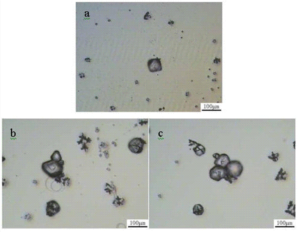
[0051] Select a boron-doped P-type Czochralski silicon single crystal with a diameter of 200 mm in crystal orientation and a resistivity of 8-12 Ω·cm. ) ratio greater than the critical value (0.2mm 2 min -1 K -1 ) grown under the conditions, so there are void-type defects in the silicon single crystal. Cut a silicon wafer on the single crystal, and make a single-sided polished Czochralski silicon wafer with a thickness of about 725 μm.

[0052] The specific steps for displaying the cavity-type defects in the above-mentioned polished Czochralski silicon wafer are:

[0053] (1) immersing the Czochralski wafer in a copper nitrate solution with a concentration of 8mol / L and a temperature of 10°C for 10 minutes to carry out copper contamination;

[0054] (2) then take out the Czochralski silicon wafer after the copper is stained, rinse the residual copper nitrate solution on the surface of the silicon wafer with deionized water, and then dry the silicon wafer;

[0055] (3) Pu...

Embodiment 2

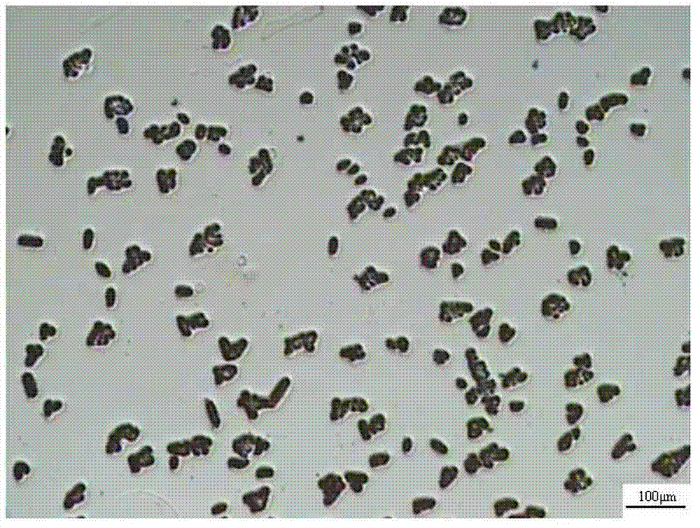
[0064] A boron-doped P-type Czochralski silicon single crystal with a diameter of 200 mm in crystal orientation and a resistivity of 8-12 Ω·cm was selected. The single crystal is when the ratio of V / G (the axial temperature gradient of crystal pulling rate / solid-liquid interface) is greater than the critical value (0.2mm 2 min -1 K -1 ) grown under the conditions, so there are void-type defects in the silicon single crystal. Cut a silicon wafer on the single crystal, and make a single-sided polished Czochralski silicon wafer with a thickness of about 725 μm.

[0065] The specific steps for displaying the cavity-type defects on the above-mentioned polished Czochralski wafer are:

[0066] (1) Immerse the Czochralski wafer in a copper nitrate solution with a concentration of 12mol / L and a temperature of 40°C for 5 minutes for copper contamination

[0067] (2) then take out the Czochralski silicon wafer after the copper is stained, rinse the residual copper nitrate solution o...

Embodiment 3

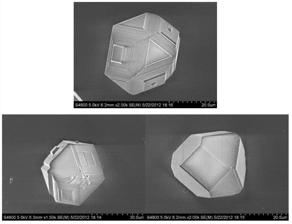
[0077] A boron-doped P-type Czochralski silicon single crystal with a diameter of 200 mm in crystal orientation and a resistivity of 8-12 Ω·cm was selected. The single crystal is when the ratio of V / G (the axial temperature gradient of crystal pulling rate / solid-liquid interface) is greater than the critical value (0.2mm 2 min -1 K -1 ) grown under the conditions, so there are void-type defects in the silicon single crystal. Cut a silicon wafer on the single crystal, and make a single-sided polished Czochralski silicon wafer with a thickness of about 725 μm.

[0078] The specific steps for displaying the cavity-type defects on the above-mentioned polished Czochralski wafer are:

[0079] (1) immersing the Czochralski wafer in a copper nitrate solution with a concentration of 4mol / L and a temperature of 25°C for 20 minutes to carry out copper contamination;

[0080](2) then take out the Czochralski silicon wafer after the copper is stained, rinse the residual copper nitrate...


PUM

PropertyMeasurementUnit
diameteraaaaaaaaaa
electrical resistivityaaaaaaaaaa
thicknessaaaaaaaaaa

Abstract

The invention provides a method for displaying and detecting void type defects in a Czochralski silicon wafer, and the void type defects are displayed by utilizing polyhedron copper precipitation. The method for displaying the void type defects in the Czochralski silicon wafer comprises the following steps of: immersing a polished silicon wafer into a copper nitrate solution for standing; rinsing the silicon wafer in deionized water, taking out and airing; performing heat treatment on the silicon wafer after copper precipitation and airing; quickly cooling the silicon wafer after heat treatment; and horizontally placing the silicon wafer after cooling in a preferential etching solution for etching. The invention further provides the method for detecting the void type defects in the Czochralski silicon wafer, and the method comprises the following steps of: preparing a silicon wafer sample according to the method; and directly observing the polished surface of the silicon wafer sample by an optical microscope or a scanning electron microscope. The polyhedron copper precipitation observed under the microscope corresponds to the void type defects. According to the method provided by the invention, the void type defects in the Czochralski silicon wafer can be clearly displayed within a shorter period of time, the observation can be conveniently performed by adopting the conventional optical microscope under common environments, and the method is suitable for detecting the void type defects in the Czochralski silicon wafer in industrial production.

Description

technical field [0001] The invention belongs to the technical field of semiconductors, in particular to a method for displaying and detecting void-type defects in Czochralski silicon wafers. Background technique [0002] Void defects are an important class of native defects in Czochralski silicon single crystals, which are formed by the accumulation of vacancies during the growth process of Czochralski silicon single crystals. If there are void-type defects in the Czochralski silicon single wafer (hereinafter referred to as: Czochralski silicon wafer) used to manufacture integrated circuits, it will lead to poor gate oxide integrity (GOI), significant PN junction leakage, and slot capacitance. problems such as short circuits and insulation failures. The existence of these problems will seriously reduce the yield of integrated circuits. Therefore, in the production of Czochralski silicon wafers, a simple and quick method is needed to display the void-type defects in silicon...

Claims


Application Information

Patent Timeline
Patent Type & Authority Applications(China)
IPC IPC(8): G01N1/28
Inventor 马向阳徐涛杨德仁
Owner ZHEJIANG UNIV
Why Eureka
Try Eureka