Process for eliminating side wall width load effect

A load effect and sidewall technology, applied in electrical components, semiconductor/solid-state device manufacturing, circuits, etc., can solve the problems of high process temperature, low output, increase device thermal budget, etc., to expand the process window and ensure electrical performance. , the effect of eliminating the load effect

Active Publication Date: 2014-12-24
SHANGHAI HUALI MICROELECTRONICS CORP
View PDF4 Cites 0 Cited by
  • Summary
  • Abstract
  • Description
  • Claims
  • Application Information

AI Technical Summary

Problems solved by technology

[0006] The traditional method to solve the load effect in the preparation of the side wall of the ON structure generally starts from two aspects of silicon nitride deposition and etching. In the silicon nitride deposition process, the method of low temperature furnace tube growth is used to deposit silicon nitride , although it can improve its deposition characteristics, so that the thickness difference of sidewall silicon nitride deposition can be close to zero, but the output per unit time is relatively low, and the process temperature is high, which will increase the thermal budget of the device (thermal budget); on the other hand It is to improve the loading effect of silicon nitride etching. By reducing the RF power of the main etching, the ion reflection bombardment effect on the pattern-intensive area can be reduced, but it can only reduce the difference in sidewall width, and cannot fundamentally eliminate the etching process. load effect

Method used


Image

  • Process for eliminating side wall width load effect
  • Process for eliminating side wall width load effect
  • Process for eliminating side wall width load effect

Examples


Embodiment Construction

[0025] The specific embodiment of the present invention will be further described below in conjunction with accompanying drawing:

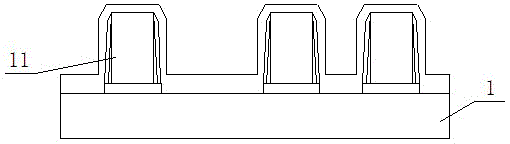
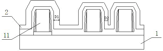
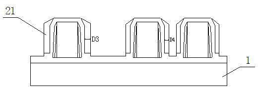
[0026] The invention is a process for eliminating the load effect of sidewall width, which is mainly applied to a semiconductor substrate provided with a gate structure, and has a pattern dense area (Dense) and a pattern empty area (Isolation) on the semiconductor substrate.

[0027] like Figure 4-7 As shown, in the silicon oxide-silicon nitride (Oxide-Nitride, ON) sidewall preparation process, the upper surface of the silicon substrate 3 is provided with a gate oxide layer 31, and the gate 33 is provided on the gate oxide 31. The silicon oxide compensation spacer 34 covers the side wall of the gate 33 and the upper surface of part of the gate oxide 31, and the silicon nitride compensation spacer 35 covers the side wall of the silicon oxide compensation spacer 34 and the gate oxide 31 remaining upper surface.

[0028] Firstly, the barrier layer...


PUM


Abstract

The invention relates to the field of semiconductor manufacture, particularly to a process for eliminating the side wall width load effect. According to the process, the conditions such as gas composition and proportion, reaction cavity pressure and radio frequency power and the like in a main etching process are adjusted to inverse the properties of the etching process so as to effectively compensate the load effect of a silicon nitride thin film in the process of chemical vapor deposition. In this way, the load effect in the side wall preparation process is finally eliminated; and the widths of the side walls formed in a figure open area and a figure dense area are close to each other, so that a process window of a device is expanded and the stable electric performance of the device is guaranteed.

Description

technical field [0001] The invention relates to the field of semiconductor manufacturing, in particular to a process for eliminating the load effect of side wall width. Background technique [0002] Due to the sidewall of the silicon oxide-silicon nitride structure (Oxide-Nitride, referred to as ON), it is mainly used to isolate the source and drain regions and the gate, so as to avoid the short channel caused by the ion implantation area of ​​the source and drain regions being too close to the gate. effect, and also has a certain protective effect on the sidewall of the gate; therefore, the sidewall etching of the silicon oxide-silicon nitride structure is a key process related to the performance of the transistor. A very critical indicator of , determines the distance between the source and drain regions and the gate, and has a great influence on the electrical properties of the device. [0003] Since the film deposition or etching rate is different in the pattern isolati...

Claims


Application Information

Patent Timeline
Patent Type & Authority Patents(China)
IPC IPC(8): H01L21/3065H01L21/02
Inventor 杨渝书李程陈玉文
Owner SHANGHAI HUALI MICROELECTRONICS CORP
Why Eureka
Try Eureka