Semiconductor layout and forming method thereof, formed semiconductor structure and method

A semiconductor and graphics technology, applied in the direction of semiconductor devices, semiconductor/solid-state device manufacturing, semiconductor/solid-state device components, etc., can solve problems such as reducing the performance of semiconductor structures, and achieve the effect of eliminating load effects and improving performance.

Pending Publication Date: 2021-11-19
SEMICON MFG INT (SHANGHAI) CORP +1
View PDF0 Cites 0 Cited by
  • Summary
  • Abstract
  • Description
  • Claims
  • Application Information

AI Technical Summary

Problems solved by technology

The pattern density of the overlay mark itself is also taken into account, especially when the overlay mark is placed inside the die (DIE), the loading effect caused by the pattern density will have a great impact on the device area of ​​the semiconductor structure, Reduces the performance of the formed semiconductor structure

Method used


Image

  • Semiconductor layout and forming method thereof, formed semiconductor structure and method
  • Semiconductor layout and forming method thereof, formed semiconductor structure and method
  • Semiconductor layout and forming method thereof, formed semiconductor structure and method

Examples


Embodiment Construction

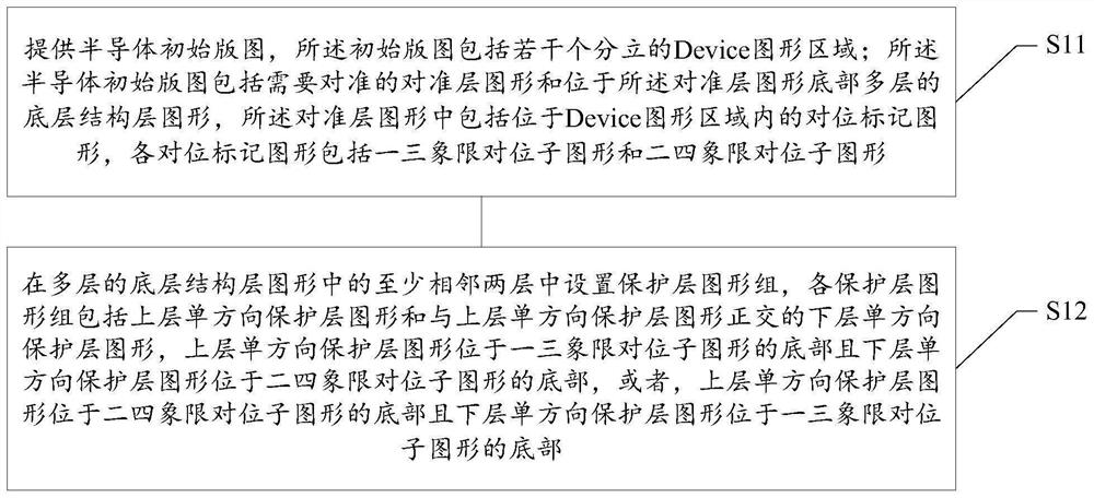
[0070] It can be seen from the background art that corresponding overlay mark patterns are provided in multiple process layers in a semiconductor structure, so as to achieve alignment between multiple process layers in a photolithography process.

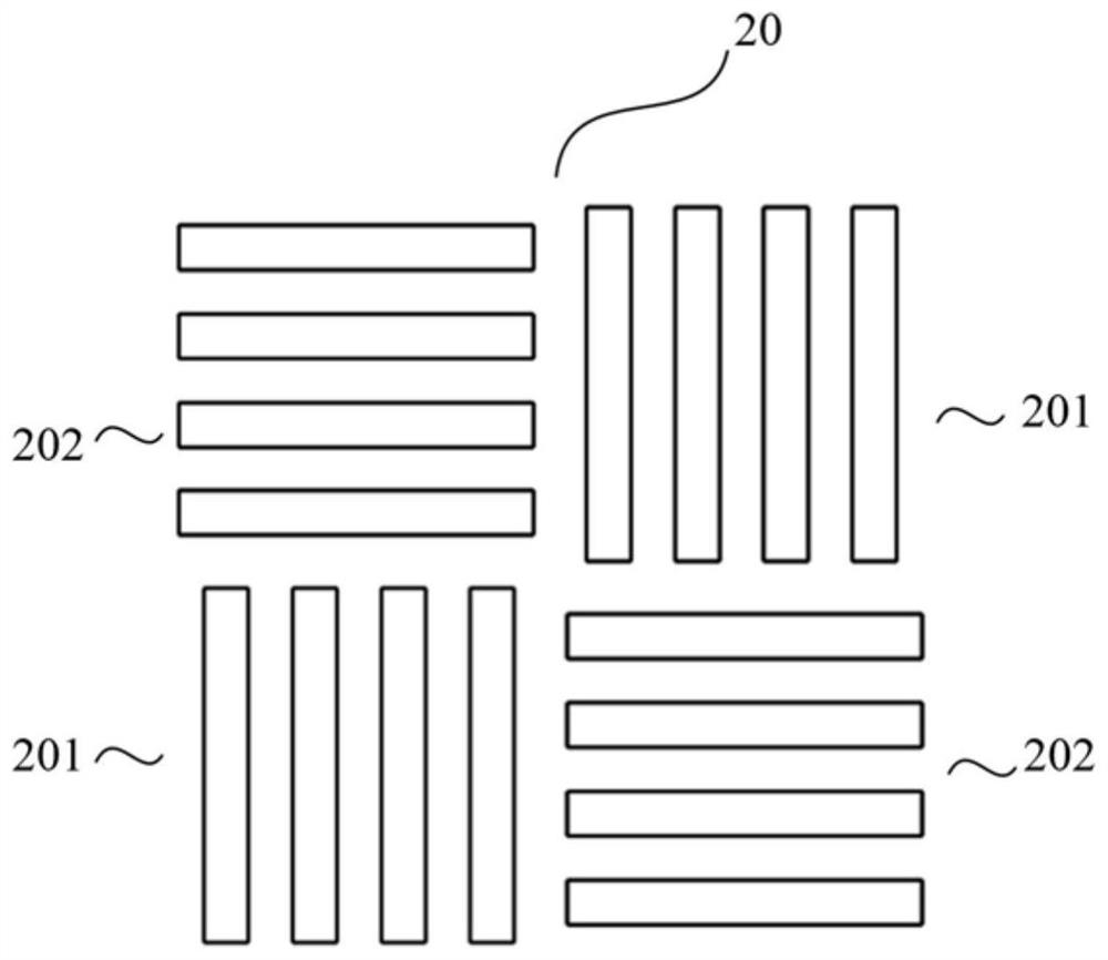
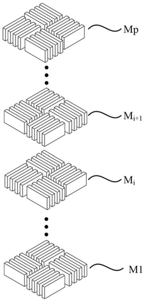
[0071] According to the light diffraction or interference theory, in order not to affect the measurement in the photolithography process, the gap (Pitch) of the protective layer pattern set in the process layer under the bottom alignment layer should be kept below 200nm, and the protection The direction of the layer pattern should be kept orthogonal to the direction of the protective layer pattern on the upper layer, that is, the protective layer pattern set in the multi-layer process layer is orthogonal to each other layer by layer from top to bottom. Since the pattern extension direction of the overlay mark is designed to exist simultaneously in the horizontal and vertical directions, the pattern extension direction of the protecti...


PUM


Abstract

The invention discloses a semiconductor layout and a forming method thereof, a formed semiconductor structure and a forming method of the semiconductor layout. The forming method of the semiconductor layout comprises the following steps: providing a semiconductor initial layout, wherein the layout comprises an alignment layer pattern needing to be aligned and a plurality layers of bottom layer structure layer patterns located at the bottom, the alignment layer pattern comprises alignment mark patterns located in a Device pattern area, and the alignment mark patterns comprise a first-quadrant and three-quadrant alignment sub-pattern and a second-quadrant and four-quadrant alignment sub-pattern; and arranging protection layer pattern groups are arranged in at least two adjacent layers in the multiple layers of bottom layer structure layer patterns, wherein each protection layer pattern group comprises an upper layer unidirectional protection layer pattern and a lower layer unidirectional protection layer pattern which is orthogonal to the upper layer unidirectional protection layer pattern. According to the scheme, the performance of the formed semiconductor structure can be improved.

Description

technical field [0001] The invention relates to the field of semiconductor integrated circuits, in particular to a semiconductor layout, a method for forming the same, and a formed semiconductor structure and method. Background technique [0002] In the semiconductor process technology, lithography technology is a crucial technology in semiconductor manufacturing technology. Photolithography technology can realize the transfer of graphics from the mask to the surface of the silicon wafer to form semiconductor products that meet the design requirements. [0003] With the reduction of chip process nodes, the requirements for overlay in the photolithography process are getting higher and higher. In order to better monitor the overlay of the device area, the size of the overlay mark is also continuously reduced, and the design requirements are getting higher and higher. The pattern density of the overlay mark itself is also taken into account, especially when the overlay mark ...

Claims


Application Information

Patent Timeline
IPC IPC(8): H01L21/027H01L21/82H01L23/544H01L27/02G03F9/00
CPCH01L27/0207H01L21/82H01L23/544H01L21/0274G03F9/7076H01L2223/54426
Inventor 张海杨晓松吴怡旻
Owner SEMICON MFG INT (SHANGHAI) CORP
Why Eureka
Try Eureka