Supercharge Your Innovation With Domain-Expert AI Agents!

Method for measuring and calculating semiconductor device well block implanted ion transverse diffusing capacity

一种扩散能力、注入离子的技术,应用在半导体/固态器件测试/测量、电气元件、电路等方向,能够解决加长制程循环时间、很难精确测定横向扩散能力等问题,达到方法简便易行的效果

Active Publication Date: 2012-11-14
SHANGHAI HUALI MICROELECTRONICS CORP
View PDF3 Cites 9 Cited by
  • Summary
  • Abstract
  • Description
  • Claims
  • Application Information

AI Technical Summary

Problems solved by technology

[0004] At present, the lateral diffusion of ions in the well area is mostly carried out through wafer acceptance test (wafer acceptance test, WAT) and electrical test. Since many subsequent processes will affect the results of WAT and electrical test, it is difficult to accurately measure its value. Lateral diffusion capability and increased process cycle time

Method used


Image

  • Method for measuring and calculating semiconductor device well block implanted ion transverse diffusing capacity
  • Method for measuring and calculating semiconductor device well block implanted ion transverse diffusing capacity
  • Method for measuring and calculating semiconductor device well block implanted ion transverse diffusing capacity

Examples


Embodiment Construction

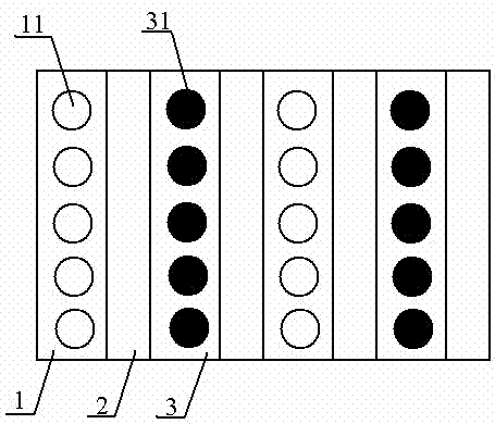
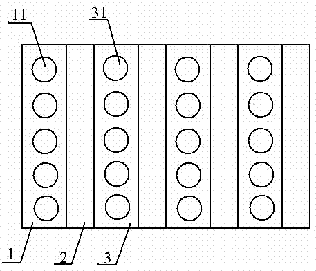
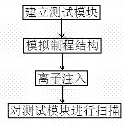
[0021] In the method for measuring the lateral diffusion ability of implanted ions in the well region of the semiconductor device according to the embodiment of the present invention, figure 1 , including the following steps:

[0022] Step 1, build a test module. Different groups of active areas (AA) with a certain area are divided on the module, for example, the size is 20umx50um. On these AAs, the P well area and the N well area are separated by intervals, and the P well and the N well are separated by shallow trench isolation (STI), and the bottom width of the STI is made different windows based on the actual process. For example, assuming that the actual STI width is 250nm, ten equal-section windows of 200 to 300 can be made respectively, and such test modules can be laid on the wafer as required. Under the premise of determining other conditions, change the conditions for measuring and calculating the ion injection in the well area.

[0023] Step 2, simulating the actu...


PUM


Abstract

The invention discloses a method for measuring and calculating semiconductor device well block implanted ion transverse diffusing capacity. The method includes that step one, a test module is established, and an active area of the module includes a P well block and an N well block which are isolated by a shallow ridge channel; step two, a processing structure is simulated, and a tungsten connecting hole of the well block is arranged; step three, an ion implanting is performed, and the P well block or the N well block is merely implanted with a first ion; and step four, the test module is subjected to scanning to obtain a continuous-tone image of the tungsten connecting hole. The method has the advantages that references for well block optimization of the semiconductor device are provided, a guarantee is provided for increasing the yield, and the method is simple, convenient and easy to practice.

Description

technical field [0001] The invention belongs to the field of semiconductors, and relates to a method for measuring ion diffusion ability, in particular to a method for measuring the lateral diffusion ability of implanted ions in the well area of ​​a semiconductor device. Background technique [0002] The quality of the well area of ​​a semiconductor device plays a key role in the semiconductor device. When the device is below 55nm, the control of the well area is especially important. There are many factors that affect the well area of ​​semiconductor devices, such as the dose, depth, angle, and ion diffusion of implanted ions. However, due to the lack of an effective evaluation method for the ion's own diffusion ability, it is difficult to control its impact on the device. [0003] The ions implanted into the well area will diffuse along the damaged lattice during the subsequent lattice repair thermal annealing process, and most of them diffuse laterally. The lateral diff...

Claims


Application Information

Patent Timeline
Patent Type & Authority Applications(China)
IPC IPC(8): H01L21/66
CPCH01L22/12
Inventor 范荣伟倪棋梁龙吟王恺陈宏璘
Owner SHANGHAI HUALI MICROELECTRONICS CORP
Features
  • R&D
  • Intellectual Property
  • Life Sciences
  • Materials
  • Tech Scout
  • Unparalleled Data Quality
  • Higher Quality Content
  • 60% Fewer Hallucinations
Learn More