

Ringing suppression circuit
A technology for suppressing circuits and series circuits, which can be applied to circuits, electrical components, and line transmission components that bypass ringing signals, and can solve problems such as disadvantages.
- Summary
- Abstract
- Description
- Claims
- Application Information
AI Technical Summary
Problems solved by technology
Method used
Image

Examples
no. 1 example )
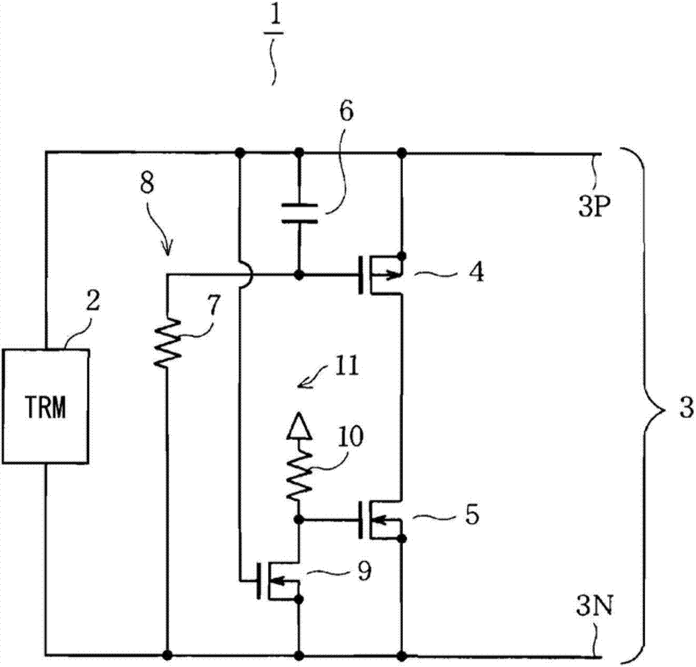
[0045] Referring to the first embodiment shown figure 1 , the ringing suppression circuit 1 is connected in parallel to the transmission line 3, and the transmission line 3 includes a transmission circuit (or receiver circuit) 2, and a high-potential-side signal line 3P and a low-potential-side signal line 3N. The ringing suppression circuit 1 includes a P-channel metal oxide semiconductor field effect transistor (MOSFET) 4 and an N-channel MOSFET 5 (first and second interline switching element).
[0046] Furthermore, a series circuit of a capacitor 6 and a resistor 7 is connected on the transmission circuit 3 , and a common connection point of each of the capacitor 6 and the resistor 7 is connected to the gate of the FET 4 . The series circuit configures the delay circuit 8 . The source (potential reference side conductive terminal) of the N-channel MOSFET 9 (inverter circuit, control switching element) is connected to the signal line 3N, the drain is pulled up to high leve...
no. 2 example )
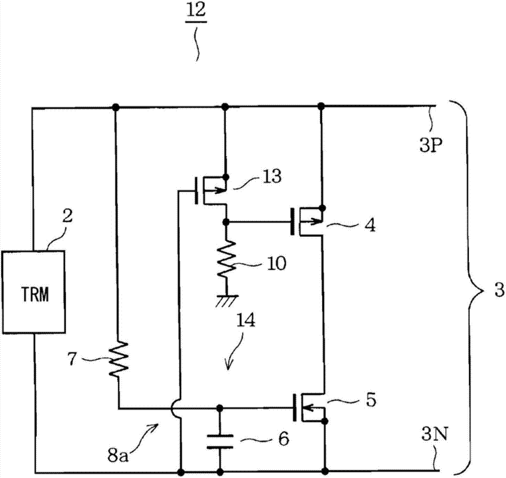
[0056] according to image 3 In the second embodiment shown, the ringing suppression circuit 12 is configured such that the on and off states of the FET 4 and the FET 5 become opposite to those of the first embodiment.
[0057] That is, the source of the P-channel MOSFET 13 (inversion circuit, control switching circuit) instead of the FET 9 is connected to the signal line 3P and the gate is connected to the signal line 3N while being lowered to the ground potential via the resistor 10, And the drain is connected to the gate of FET 4 . Further, the gate of the FET 5 is connected to the signal line 3N via the capacitor 6 while also being connected to the signal line 3P via the resistor 7 . In addition, a series circuit composed of a resistor 7 and a capacitor 6 configures a delay circuit 8a. Furthermore, the delay circuit 8 a and the FET 13 configure a control circuit (control section) 14 .
[0058] In the second embodiment, when the differential signal is high, FET 13 is on ...
no. 3 example )
[0062] according to Figure 4 In the third embodiment shown, the ringing suppression circuit 15 configures the delay circuit 17 by connecting the diode 16 in parallel to the resistor 7 in the ringing suppression circuit 1 of the first embodiment. Further, the gate of the FET 9 is also connected to the signal line 3P via the resistor 18 while being connected to the signal line 3N via the capacitor 19 . Diode 16 is connected in parallel to resistor 18 .
[0063] Here, FET 9 , resistors 10 and 18 , capacitor 19 , and diode 20 configure an inverter circuit 21 . Here, the diode 16 is connected so that the anode is on the signal line 3P side and the diode 20 is connected so that the anode is on the signal line 3N side. Furthermore, the delay circuit 17 and the inverter circuit 21 configure a control circuit (control section) 22 .
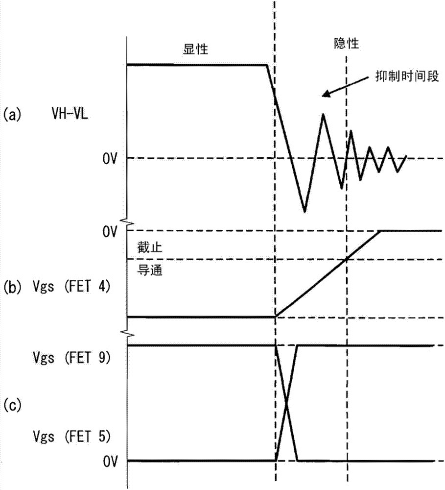
[0064] In the first embodiment, if an overshoot occurs after the signal waveform falls when the differential signal level changes from high to low, th...
PUM
 Abstract
Description
Claims
Application Information