Thermosetting resin composition, dry film and printed circuit board (pcb)
A resin composition, thermosetting technology, applied in printed circuit components, printed circuit secondary treatment, circuit substrate materials, etc., can solve the problems of poor appearance, reduced covering of solder resist, etc., to achieve excellent covering, prevent bad appearance effect
- Summary
- Abstract
- Description
- Claims
- Application Information
AI Technical Summary
Problems solved by technology
Method used
Image
Examples
no. 1 approach
[0038] First, a first embodiment of the present invention will be described.
[0039] The thermosetting resin composition according to the first embodiment of the present invention is a composition containing (A) epoxy resin, (B) colorant, and (C) curing agent as essential components, and is characterized in that (B) colorant Use colorants with specific absorbance peaks and absorption wavelengths for this.
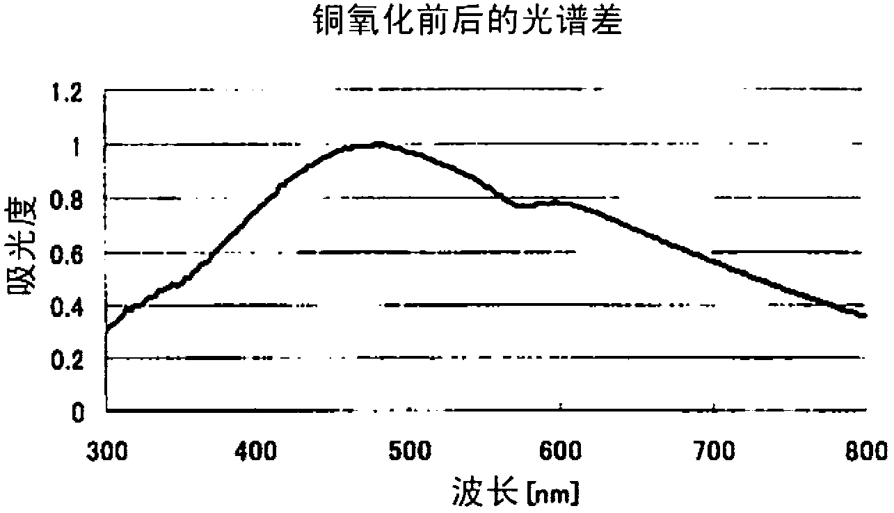
[0040] Specifically, as the (B) colorant, a colorant having an absorbance peak at a specific wavelength suitable for covering oxidation of a copper circuit and absorbing at an oscillation wavelength of a laser used for laser processing is used. The above specific wavelength regions such as figure 1 As shown, when the difference in the absorbance spectrum before and after the oxidation of the copper forming the circuit pattern is taken, it corresponds to two wavelength ranges where the intensity is strong. Therefore, by making the (B) colorant have an absorbance peak in ...
no. 2 approach
[0085] Next, a second embodiment of the present invention will be described.
[0086] The dry film according to the second embodiment of the present invention is a dry film provided with a dry coating film on a carrier film, and the dry coating film is laminated and thermally cured on a substrate on which a circuit pattern made of copper is formed to form a printed circuit board. circuit board.
[0087] The dry coating film in the dry film of this embodiment has a lower layer for suppressing the oxidation of copper that covers the circuit pattern, and an upper layer of one or more layers for laser processing and copper circuit covering (hereinafter, Each layer is referred to as an "upper layer" when it includes one layer or two or more layers.) In the laminated structure formed, the lower layer is a layer formed of a composition containing (a) epoxy resin and (b) phenolic resin. By forming the lower layer covering the circuit pattern as a layer having a function of suppressin...
Embodiment 1
[0122] Each component shown in the following table|surface was blended, premixed with the mixer, and kneaded using the three-roll mill, and the thermosetting resin composition of each Example and the comparative example was prepared.
[0123] Table 1
[0124]
[0125] *1-1) Bisphenol A type liquid epoxy resin (liquid at 20°C) (manufactured by Mitsubishi Chemical Corporation, epoxy equivalent 184~194)
[0126] *1-2) Resorcinol-type epoxy resin (manufactured by Nagase ChemteX Corporation, epoxy equivalent 117)
[0127] *1-3) Naphthol-type epoxy resin (manufactured by DIC CORPORATION, epoxy equivalent 135~165)
[0128] *1-4) Cyclohexanone solution with a solid content of 60% of cresol novolak type epoxy resin (manufactured by DIC CORPORATION, epoxy equivalent 200~230)
[0129] *1-5) Phenol novolac resin (manufactured by DIC CORPORATION, s.p.78~82°C) cyclohexanone solution with a solid content of 60%
[0130] *1-6) Cyclohexanone solution with 30% solid content of phenoxy r...
PUM
| Property | Measurement | Unit |
|---|---|---|
| The average particle size | aaaaa | aaaaa |
| Thickness | aaaaa | aaaaa |
| Thickness | aaaaa | aaaaa |
Abstract
Description
Claims
Application Information


