Liquid crystal display panel and manufacturing method thereof

A technology for a liquid crystal display panel and a manufacturing method, which is applied in the directions of nonlinear optics, instruments, optics, etc., can solve the problems of complicated liquid crystal display panel manufacturing process, inability to cure the sealant 207, high manufacturing cost of liquid crystal display panel, etc.

Inactive Publication Date: 2012-11-28
TCL CHINA STAR OPTOELECTRONICS TECH CO LTD
View PDF4 Cites 24 Cited by
  • Summary
  • Abstract
  • Description
  • Claims
  • Application Information

AI Technical Summary

Problems solved by technology

In this case, it is necessary to make the distance L3 as small as possible, and to use the ultraviolet light source 10 to irradiate the sealant 207, and to prevent the liquid crystal layer 203 from being irradiated by the ultraviolet light source 10, so that the thin film transistor array substrate 202 and The technical solution of placing the ultraviolet mask 201 between the ultraviolet light sources 10 can no longer solve the technical problems of curing the frame glue 207 and preventing the liquid crystal from being damaged
[0006] In addition, if the ultraviolet mask 201 is to be applied to the manufacturing process of the liquid crystal display panel, the ultraviolet mask 201 needs to be made according to the product actually used, and, in the manufacturing process of the liquid crystal display panel, the ultraviolet mask 201 also needs to be Accurate alignment with the LCD panel, otherwise the above purpose will not be achieved
The above technical solution makes the liquid crystal display panel have a relatively high manufacturing cost, and complicates the manufacturing process of the liquid crystal display panel

Method used


Image

  • Liquid crystal display panel and manufacturing method thereof
  • Liquid crystal display panel and manufacturing method thereof
  • Liquid crystal display panel and manufacturing method thereof

Examples


Embodiment Construction

[0025] The following descriptions of the various embodiments refer to the accompanying drawings to illustrate specific embodiments in which the present invention can be practiced.

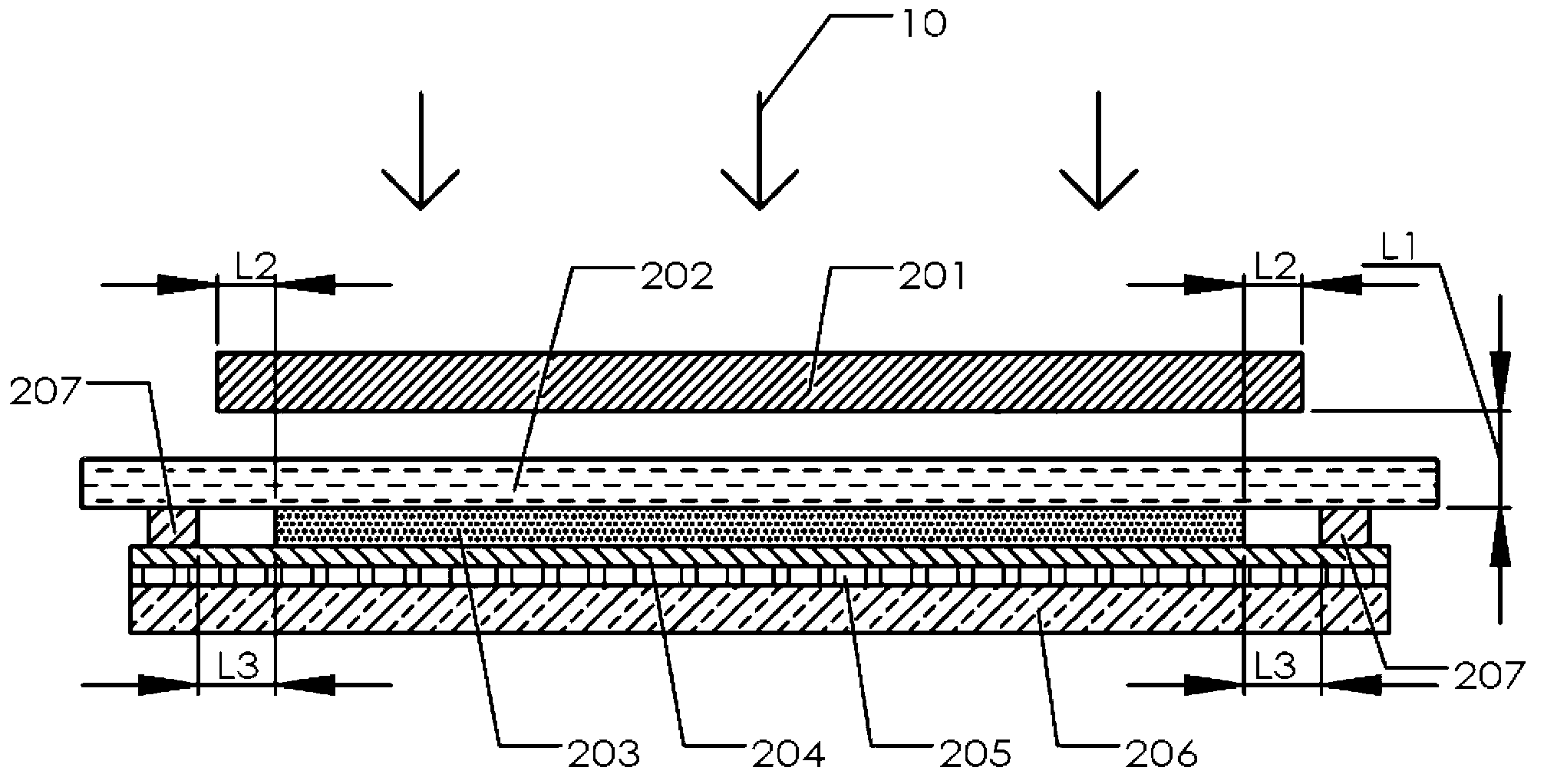
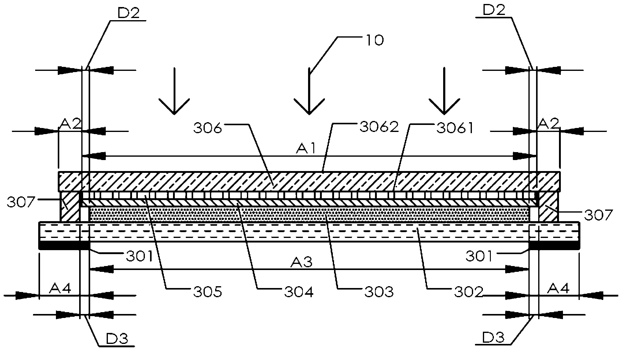
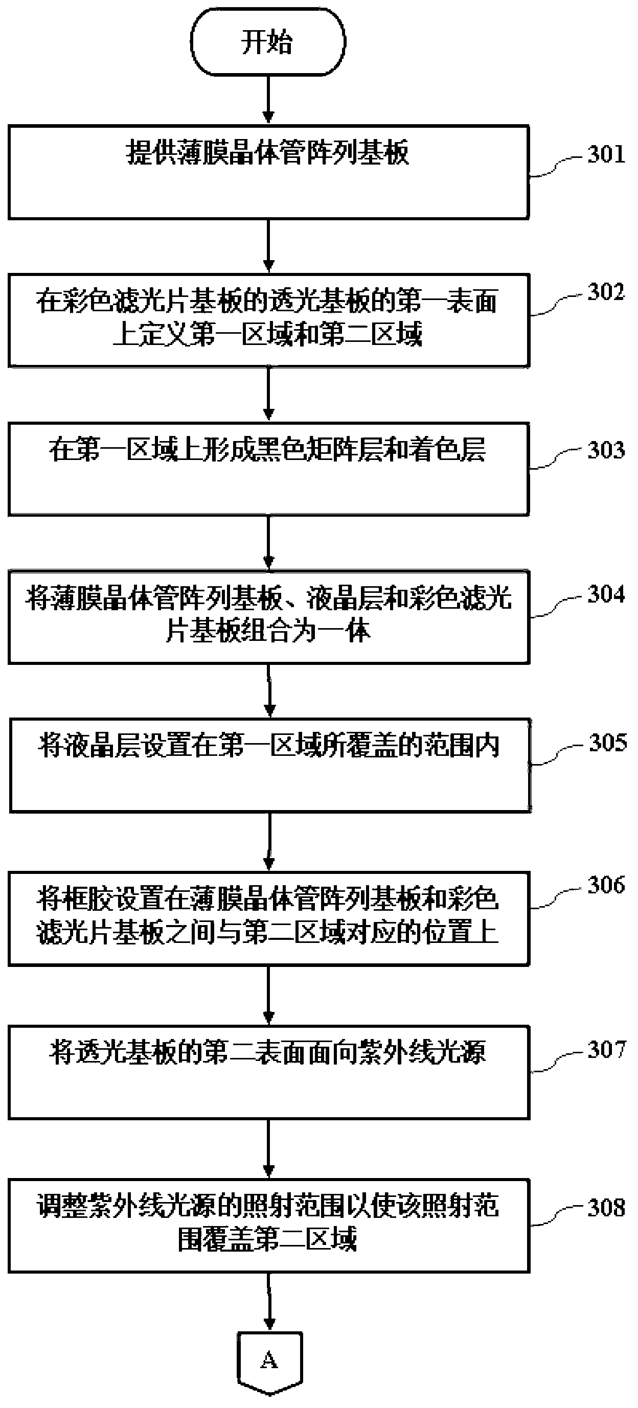
[0026] refer to figure 2 , figure 2It is a schematic diagram of the curing method of the sealant in the liquid crystal display panel of the present invention. The liquid crystal display panel of the present invention includes: a thin film transistor array substrate 302, a color filter substrate, a liquid crystal layer 303 and a frame. Wherein, the color filter substrate includes a transparent substrate 306 , a black matrix layer 305 and a colored layer 304 , and the transparent substrate 306 may be a glass substrate. The transparent substrate 306 has a first surface 3061 and a second surface 3062, the first surface 3061 is provided with a first area A1 and a second area A2, the second area A2 is located outside the first area A1, the black matrix layer 305 and the colored The layer 304 is disp...


PUM


Abstract

The invention discloses a liquid crystal display panel, which comprises a thin-film transistor array substrate, a color filter substrate, a liquid crystal layer and a frame, wherein the color filter substrate comprises a light transmission substrate, a black matrix layer and a colored layer, the light transmission substrate is provided with a first area and a second area, and the black matrix layer and the colored layer are arranged in the first area; the liquid crystal layer is arranged between the thin-film transistor array substrate and the color filter substrate; and the frame is arranged between the thin-film transistor array substrate and the color filter substrate and corresponds to the second area. The invention also discloses a manufacturing method of the liquid crystal display panel. An ultraviolet light source is shielded by the black matrix layer and the colored layer, so that in the process by utilizing the ultraviolet light source to solidify a rubber frame, an ultraviolet mask can be omitted.

Description

【Technical field】 [0001] The invention relates to the technical field of liquid crystal display panels, in particular to a liquid crystal display panel and a manufacturing method thereof. 【Background technique】 [0002] During the manufacturing process of the liquid crystal display panel, the sealant needs to be cured. Such as figure 1 As shown, the traditional technical means for curing the frame glue 207 is: facing the thin film transistor array substrate 202 of the liquid crystal display panel to the ultraviolet light source 10, and placing an ultraviolet mask (Ultraviolet Mask) between the thin film transistor array substrate 202 and the ultraviolet light source 10 ) 201 , using the ultraviolet light source 10 to irradiate the sealant 207 on the side of the thin film transistor array substrate 202 , and using the ultraviolet mask 201 to shield the active area (Active Area) in the liquid crystal display panel. [0003] The purpose of irradiating the sealant 207 with the...

Claims


Application Information

Patent Timeline
Patent Type & Authority Applications(China)
IPC IPC(8): G02F1/1335G02F1/1339G02F1/1333G02F1/1362
CPCG02F1/133308G02F1/1339G02F1/1341G02F1/133512G02F1/133388G02F1/133514G02F1/1368
Inventor 陈世烽许哲豪施明宏李征华
Owner TCL CHINA STAR OPTOELECTRONICS TECH CO LTD
Why Eureka
Try Eureka