Gate driving circuit

A gate drive circuit, gate drive technology, used in instruments, static indicators, etc., to achieve the effect of reducing size and strong output capability

Active Publication Date: 2012-11-28
KUSN INFOVISION OPTOELECTRONICS
View PDF6 Cites 38 Cited by
  • Summary
  • Abstract
  • Description
  • Claims
  • Application Information

AI Technical Summary

Problems solved by technology

[0006] The object of the present invention is to provide a gate drive circuit to solve the problem of the pull-up of the gate drive circuit in the miniaturization of existing liquid crystal display devices and the development of high resolution The problem of insufficient transistor output capability

Method used


Image

  • Gate driving circuit
  • Gate driving circuit
  • Gate driving circuit

Examples


Embodiment 1

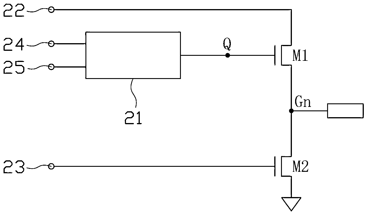
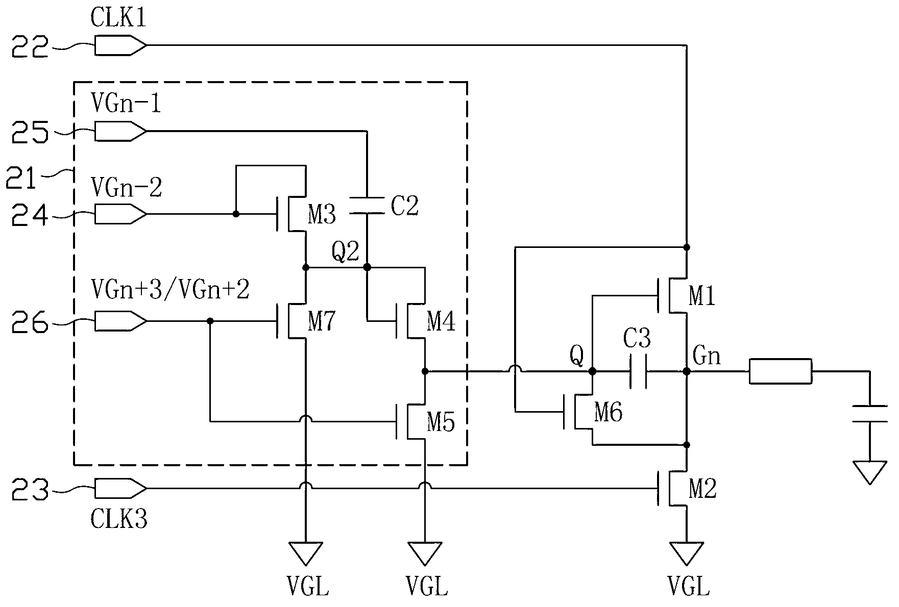
[0051] figure 2 It is a circuit diagram of the gate driving sub-circuit according to Embodiment 1 of the present invention. See figure 2 , which plots the figure 1 The specific circuit structure of the middle latch 21, and this embodiment is a preferred implementation mode of the present invention. The gate driving sub-circuit of this embodiment includes a latch 21 , a pull-up switch element M1 , a pull-down switch element M2 , a pull-up capacitor C3 and a sixth switch element M6 . The first control end of the pull-up switching element M1 is connected to the latch output Q of the latch 21, the first input end of the pull-up switching element M1 is connected to the first timing signal input end 22, and the first pull-up switching element M1 The output terminal serves as the output terminal Gn of the gate driving sub-circuit. The second control end of the pull-down switch element M2 is connected to the second timing signal input end 23, the second output end of the pull-d...

Embodiment 2

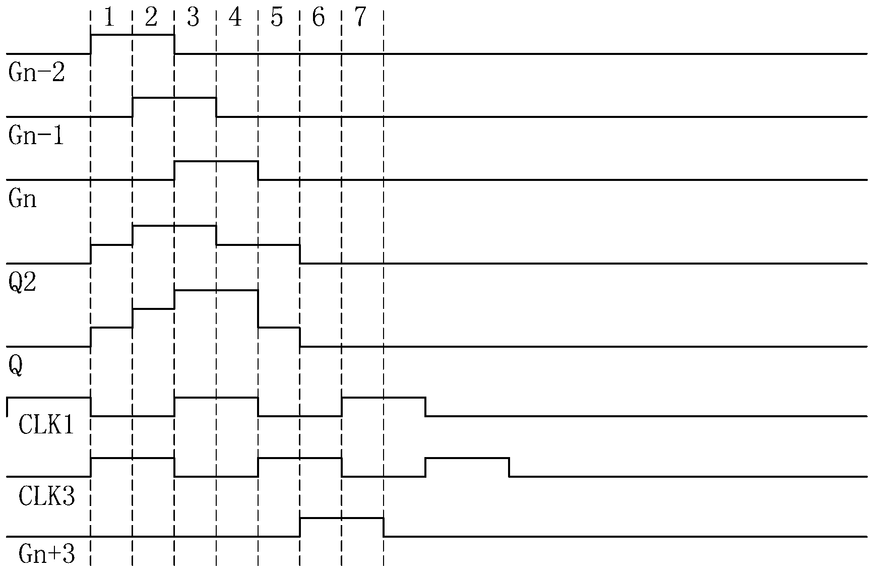
[0073] See Image 6 , which is a circuit diagram of the gate drive circuit in Embodiment 2 of the present invention, and figure 2 The difference is that the figure 2 In the seventh switch element M7, and the third control terminal of the third switch element M3 receives the CLK3 signal input from the second timing signal input terminal 23 ( figure 2 The third control end of the third switch element M3 is connected to the first pull-up signal input end 24). Depend on image 3 As can be seen from the waveform diagram shown in , when the Gn-2 signal is at a high level, the CLK3 signal is also at a high level, so this embodiment can turn on the third switching element M3 at the same time (that is, stage 1), In order to make the first pull-up signal VGn-2 pull up the voltage of point Q for the first time. And the circuit is more concise after the seventh switching element M7 is omitted. Other circuit structures and working principles of this embodiment are the same as fig...

Embodiment 3

[0075] See Figure 7 , which is a circuit diagram of the gate drive sub-circuit in Embodiment 3 of the present invention, and figure 2 The only difference is that the figure 2 The sixth switching element M6 in. The function of the sixth switch element M6 is to transfer the voltage at the stable point Q to the gate drive sub-circuit when the CLK1 high-level signal input by the first timing signal input terminal 22 is output to the output terminal Gn of the gate drive sub-circuit through the third switch element M3. The pole drives the output terminal Gn of the sub-circuit, thereby stabilizing the voltages of the Q point and the Gn point, and also improving the stability of the circuit. It can be seen that the sixth switching element M6 is not a necessary element in the present invention. In the absence of the sixth switching element M6, the circuit of this embodiment can also realize the third switching of the voltage at point Q at the output terminal of the latch 21. leve...


PUM


Abstract

The invention discloses a gate driving circuit which comprises a plurality of gate driving sub-circuits, wherein each gate driving sub-circuit comprises an upward-pull switch element, a downward-pull switch element and a latch; and the latch is used for respectively carrying out first-stage upward pull and second-stage upward pull on voltage output from the output end of the latch through a first upward pull signal and a second upward pull signal which are respectively input from a first upward pull signal input end and a second upward pull signal end so as to improve a control signal output from the latch to a first control end of the upward-pull switch element. According to the invention, the latches can output very high voltage to the upward-pull switch elements in a time period in which the gate driving sub-circuits output gate voltage, and then the output capability of the upward-pull switch element is improved, so that the sizes of the upward-pull switch elements can be further decreased on the premise of outputting enough gate voltage, therefore, the gate driving circuit is specifically suitable for meeting the design requirements of small-panel liquid crystal display devices.

Description

technical field [0001] The invention relates to a driving circuit, in particular to a grid driving circuit suitable for a liquid crystal display device. Background technique [0002] Liquid Crystal Display (LCD) has many advantages such as lightness, lightness, energy saving, and no radiation, so it has gradually replaced the traditional cathode ray tube (CRT) display. At present, liquid crystal displays are widely used in high-definition digital televisions, desktop computers, personal digital assistants (PDAs), notebook computers, mobile phones, digital cameras and other electronic equipment. [0003] Taking a thin film transistor (Thin Film Transistor, TFT) liquid crystal display device as an example, it includes: a liquid crystal display panel and a driving circuit, wherein the liquid crystal display panel includes a plurality of gate lines and a plurality of data lines, and two adjacent gate lines The polar line intersects two adjacent data lines to form a pixel unit,...

Claims


Application Information

Patent Timeline
Patent Type & Authority Applications(China)
IPC IPC(8): G09G3/36
Inventor 鲁佳浩李全虎
Owner KUSN INFOVISION OPTOELECTRONICS
Why Eureka
Try Eureka