Manufacturing method for embedding copper heat sink into circuit board

A technology of copper heat sink and manufacturing method, which is applied in the field of circuit board manufacturing, can solve problems such as low production capacity and difficulty in meeting mass production requirements, and achieve the effects of reducing manpower, facilitating inlay operations, and small bending deformation

Active Publication Date: 2014-12-17
KALEX MULTI LAYER CIRCUIT BOARD (ZHONGSHAN) CO LTD
View PDF4 Cites 0 Cited by
  • Summary
  • Abstract
  • Description
  • Claims
  • Application Information

AI Technical Summary

Problems solved by technology

[0003] The patent number is ZL200910041004.3, and the application date is July 9, 2009. In a circuit board manufacturing method, the copper lamination process is designed for manual operation. Pressing not only requires a lot of manpower, but also has low production capacity, making it difficult to meet mass production requirements

Method used


Image

  • Manufacturing method for embedding copper heat sink into circuit board
  • Manufacturing method for embedding copper heat sink into circuit board
  • Manufacturing method for embedding copper heat sink into circuit board

Examples


Embodiment

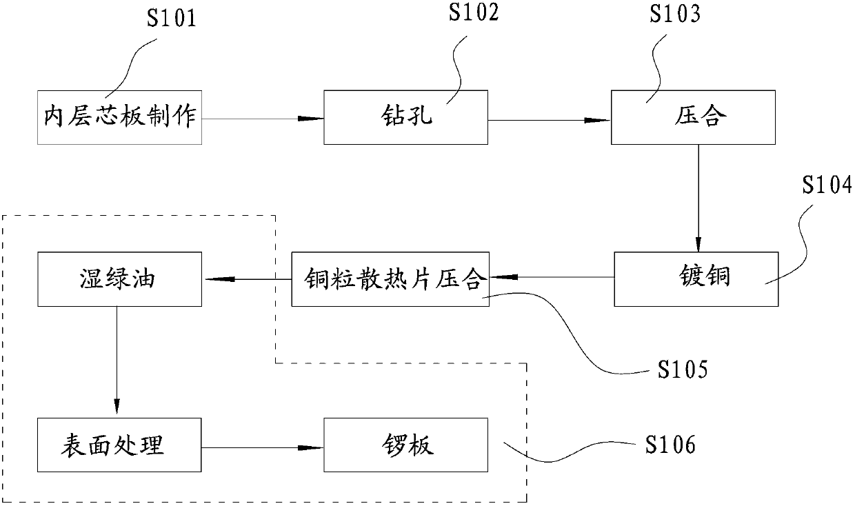
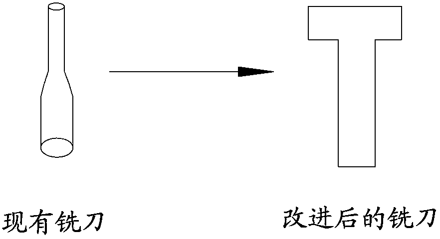
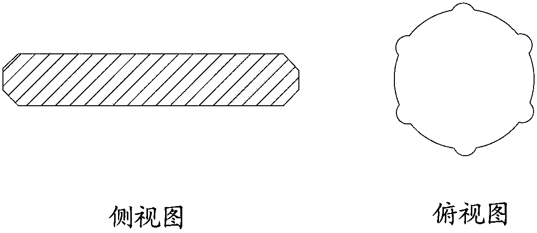
[0025] Take copper heat sinks with diameters of 8.2±0.005mm and 10.2±0.005mm embedded on a 1.7mm thick PCB as an example. figure 1 It is a complete circuit board manufacturing process flow adopted in this embodiment. figure 2 It is a comparison diagram of milling cutter structure before and after improvement in the embodiment of the present invention. image 3 It is a schematic diagram of the structure of the copper heat sink embedded in the circuit board in the embodiment of the present invention, and the diameter of the copper heat sink can be between 8mm-12mm. The diameters of the copper cooling fins used in this embodiment are 8.2±0.005mm and 10.2±0.005mm.

[0026] The following combination figure 1 , describe the embodiment of the present invention in detail, wherein the production of the inner layer core board, wet green oil, and surface treatment are traditional processes. Here, only a brief overview of the method used in this example is given, but it is not limited ...


PUM


Abstract

The invention discloses a manufacturing method for embedding a copper heat sink into a circuit board, which comprises the following steps of: a drilling process: drilling a copper heat sink embedding hole on a circuit board subjected to pressing treatment, wherein the rotating speed of a drill bit is controlled to be 20000 revolutions / minute, the board inlet speed is controlled to be 10 inches / minutes, and the board withdraw speed is controlled to be 100 inches / minutes; and an embedding process: installing a milling cutter with a cylindrical end on a milling machine, fixing the circuit board with the copper heat sink embedding hole on the milling machine, placing the copper heat sink into the copper heat sink embedding hole, starting the milling machine, and moving the milling cutter to the copper heat sink required to be pressed, so that the milling cutter presses the copper heat sink downwards in a non-rotating speed mode until a copper sheet is completely embedded into the circuit board. According to the invention, the automation of the embedding pressing process of copper heat sinks can be realized, thereby reducing manpower, increasing the productivity and meeting the mass production requirements.

Description

technical field [0001] The invention relates to the technical field of circuit board manufacturing, in particular to a manufacturing method for embedding copper heat sinks into a circuit board. Background technique [0002] With the rapid development of modern electronic technology, more and more integrated chips are used in complex circuit design. At the same time, the trend of circuit board integration has been set. For some high-power components assembled on circuit boards, how to dissipate heat becomes a big problem. subject. The usual situation is to mount heat sinks on the surface of the heating element. Although this design solves the problem of heat dissipation, it greatly increases the volume of the finished product, which is not conducive to the high integration of products and the design requirements of high-layer boards. In order to reduce the volume of the product and achieve a good heat dissipation effect, a concept of embedding copper sheets in the circuit bo...

Claims


Application Information

Patent Timeline
Patent Type & Authority Patents(China)
IPC IPC(8): H05K3/30
Inventor 黄杏娇陈德泉
Owner KALEX MULTI LAYER CIRCUIT BOARD (ZHONGSHAN) CO LTD
Why Eureka
Try Eureka