
Eureka
For R&D, Eureka makes reading and utilizing patents & technical documents easy.
Eureka AIR
Designed for self-driven R&D workflows. Generate viable solutions, solve complex R&D challenges, empower your innovation with AI.

Eureka Materials
Designed for material experts only. Revolutionize your material R&D, from search, analyze, to developing new materials.

TechResearch
Generate reliable direction feasibility study reports for your R&D in just a few steps.

TechSeek
Discover and master advanced knowledge NOW. Basics, ideas, possibilities, all at once.

TechMind
As an expert in R&D Theories, TechMind can generates customized viable solutions instantly.

TechRisk
Analyze your overall solution with one click, know your potential R&D risks in advance.

TechMonitor
Get weekly tech updates, stay abreast of the latest tech innovations and key insights.
Piezoelectric thin-film element, process for producing same, and piezoelectric thin-film device
A piezoelectric film and device technology, applied in the manufacture/assembly of piezoelectric/electrostrictive devices, piezoelectric devices/electrostrictive devices, material selection for piezoelectric devices or electrostrictive devices, etc., can Solve the problems of characteristic deviation deterioration, the influence of size cannot be ignored, etc., and achieve the effect of excellent piezoelectric characteristics
- Summary
- Abstract
- Description
- Claims
- Application Information
AI Technical Summary
Problems solved by technology
Method used
Image

Examples
Embodiment 1
[0115] Embodiments of the present invention are described below.
Embodiment 1)
[0117] use Figure 1~Figure 8 illustrate.
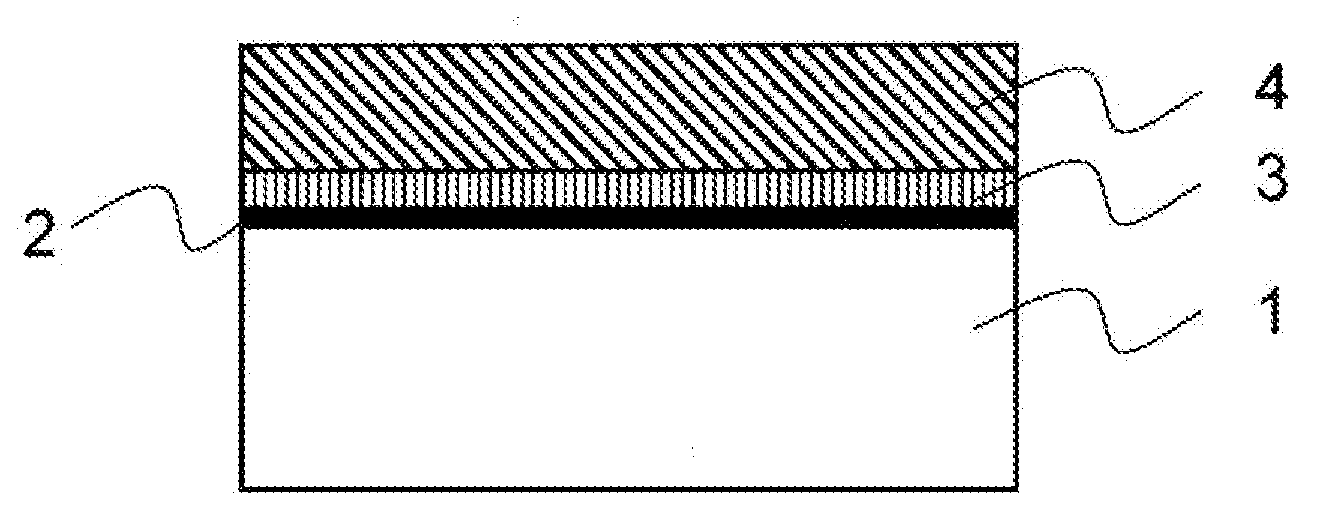
[0118] figure 1 A cross-sectional view showing an overview of a substrate with a piezoelectric thin film. In this embodiment, an adhesive layer 2 is formed on a Si substrate 1 having an oxide film, and a lower electrode layer 3 and a piezoelectric thin film layer 4 of KNN with a perovskite structure are sequentially formed on the upper portion of the adhesive layer 2. Piezoelectric thin film devices.
[0119] At this time, the crystal system of the piezoelectric film layer 4 is quasi-cubic or tetragonal or orthorhombic, and at least a part of the piezoelectric film layer 4 can be ABO 3 crystalline or amorphous or a mixture of the two. Here, A is one or more elements selected from Li, Na, K, La, Sr, Nd, Ba, and Bi, and B is an element selected from Zr, Ti, Mn, Mg, Nb, Sn, Sb, Ta, and One or more elements in In, O is oxygen. Pb-containing piezoelectric material may be used as the A-site piezoelectric material, but a Pb-free piez...
Embodiment 2)
[0144] use Figure 9~Figure 10 illustrate.
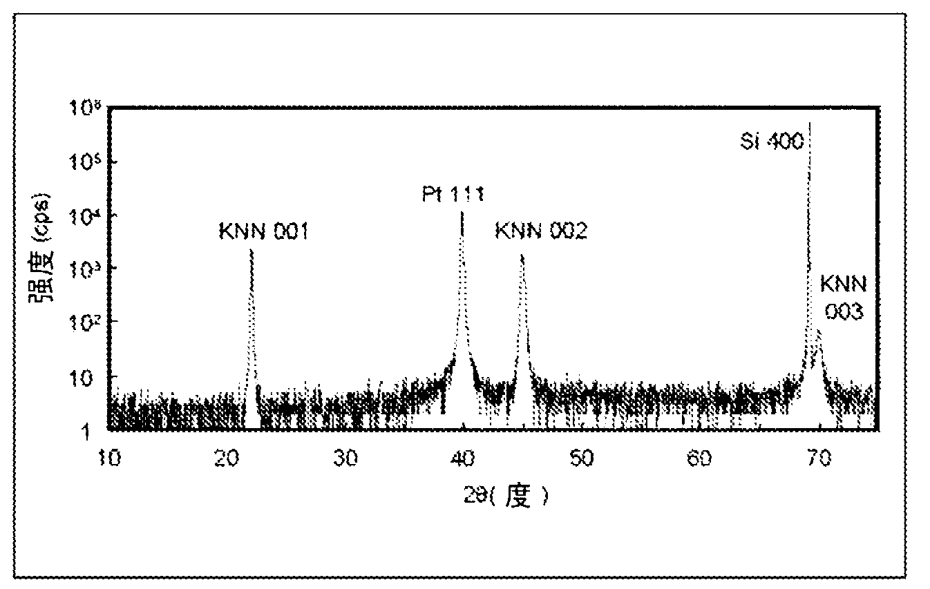
[0145] Next, when accurately calculating the diffraction intensity ratio of the (001) orientation component and the (111) orientation component, it is necessary to discuss the correction values of the respective X-ray diffraction intensities. For this purpose, the pole figures of (001) and (111) are investigated.
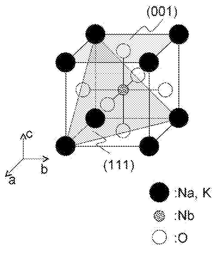
[0146] Figure 9 Displays the simulation results for the pole figure. Figure 9 (a) is a simulation result of a pole figure with (001) as a pole. As shown in this figure, it can be seen that the (110) diffraction of the (001) oriented KNN contributes 4 equivalent diffractions. At this time, the correction factor is considered to be 4. On the other hand, by Figure 9 (b) The simulation results using (111) as the pole figure, it can be seen that the (110) diffraction of the (111)-oriented KNN contributes 3 equivalent diffractions, so the correction factor is 3. Therefore, when the volume fraction of (001) orientati...
PUM
| Property | Measurement | Unit |
|---|---|---|
| thickness | aaaaa | aaaaa |
| thickness | aaaaa | aaaaa |
| thickness | aaaaa | aaaaa |
Abstract
Description
Claims
Application Information
 - R&D Engineer
- R&D Manager
- IP Professional
- Industry Leading Data Capabilities
- Powerful AI technology
- Patent DNA Extraction
Browse by: Latest US Patents, China's latest patents, Technical Efficacy Thesaurus, Application Domain, Technology Topic, Popular Technical Reports.
© 2024 PatSnap. All rights reserved.Legal|Privacy policy|Modern Slavery Act Transparency Statement|Sitemap|About US| Contact US: help@patsnap.com