Thin film strip structure, solar cell and manufacturing method of thin film strip structure

A manufacturing method and strip-shaped technology, which is applied in the fields of final product manufacturing, sustainable manufacturing/processing, semiconductor/solid-state device manufacturing, etc., can solve problems such as film damage, irregular crack damage to semiconductor substrates, etc., to reduce recombination, reduce Effect of small recombination current and large effective area

A manufacturing method and strip-shaped technology, which is applied in the fields of final product manufacturing, sustainable manufacturing/processing, semiconductor/solid-state device manufacturing, etc., can solve problems such as film damage, irregular crack damage to semiconductor substrates, etc., to reduce recombination, reduce Effect of small recombination current and large effective area

CN102832116BActive Publication Date: 2015-03-25盐城新汇村镇建设发展有限公司

Image

  • Thin film strip structure, solar cell and manufacturing method of thin film strip structure
  • Thin film strip structure, solar cell and manufacturing method of thin film strip structure
  • Thin film strip structure, solar cell and manufacturing method of thin film strip structure

Examples


Embodiment Construction

[0029] Embodiments of the present invention are described in detail below, examples of which are shown in the drawings, wherein the same or similar reference numerals designate the same or similar elements or elements having the same or similar functions throughout. The embodiments described below by referring to the figures are exemplary only for explaining the present invention and should not be construed as limiting the present invention.

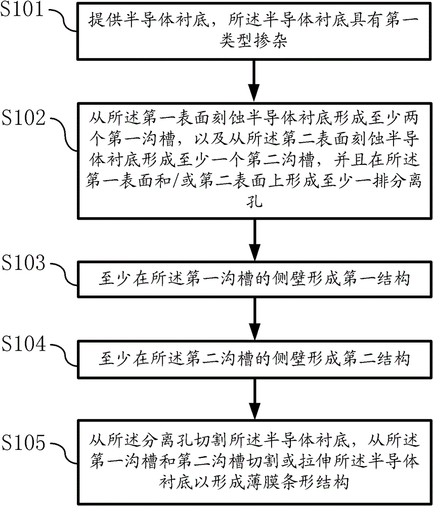
[0030] Such as image 3 Shown is a flowchart of a method for forming a thin film strip structure according to an embodiment of the present invention, including the following steps:

[0031] Step S101, providing a semiconductor substrate, the semiconductor substrate 101 has a second doping type or no doping, the semiconductor substrate 101 includes a first surface 101-1 and a second surface 101-2 opposite thereto, refer to Figure 4 , 5. In one embodiment of the present invention, the semiconductor substrate 101 is single crystal silico...


PUM

PropertyMeasurementUnit
thicknessaaaaaaaaaa
widthaaaaaaaaaa
thicknessaaaaaaaaaa

Abstract

The invention provides a thin film strip structure, a manufacturing method the thin film strip structure, and a thin film strip structure array. The manufacturing method of the thin film strip structure comprises the following steps: providing a semiconductor substrate; forming at least one dent or a row of separating holes on a first surface and / or a second surface of the semiconductor substrate; etching the semiconductor substrate from the first surface to form at least two first grooves, and etching the semiconductor substrate from the second surface to form at least one second groove; and separating the semiconductor substrate from the dent or the separating holes, and cutting or stretching the semiconductor substrate from the first grooves and the second grooves to form the thin film strip structure. With the adoption of the thin film strip structure, the damage to the strip structure and the thin film when separating the thin film strip structure from the semiconductor substrate can be effectively reduced, and the production rate can be increased. The thin film strip structure and the manufacturing method of the thin film strip structure also can save the semiconductor material and reduce the manufacturing cost.

Description

technical field [0001] The invention relates to a semiconductor process, in particular to a novel, high-efficiency, low-cost thin film strip structure and a manufacturing method of a solar cell. Background technique [0002] The thin film strip structure is prepared into a semiconductor device with a layer of thin film, which uses very little semiconductor material, so it is easier to reduce the cost. For the typical application of thin film strip structure - thin film solar cell, it is not only a high-efficiency energy product, but also can be used as a new type of building material, which is easier to realize the perfect combination with the building. Under the background of continuous shortage of silicon raw materials in the international market, thin-film solar cells have become a new trend and new hotspot in the development of the international photovoltaic market. At present, there are three main types of thin-film batteries that can be industrialized and mass-produce...

Claims


Application Information

Patent Timeline
25 Mar 2015
Publication
CN102832116B
IPC
H01L21/301; H01L31/18; H01L31/0224; H01L31/042
CPC
Y02E10/50; Y02P70/50
Inventors
朱慧珑; 骆志炯