IGBT (insulated gate bipolar translator) module packaging process and IGBT module with bidirectional heat radiation

A two-way heat dissipation and module packaging technology, which is applied in the IGBT module packaging process and the field of IGBT modules with two-way heat dissipation, can solve problems such as temperature rise, high-power IGBT chip damage, and poor heat dissipation, so as to improve heat dissipation and chip efficiency. , The effect of improving the heat dissipation capacity

Inactive Publication Date: 2012-12-19
淄博美林电子有限公司
View PDF3 Cites 2 Cited by
  • Summary
  • Abstract
  • Description
  • Claims
  • Application Information

AI Technical Summary

Problems solved by technology

[0002] like Figure 9 As shown, the traditional insulated gate bipolar transistor IGBT module packaging adopts the method of punching metal wires 7 to connect the chips in parallel and in series to achieve the purpose of increasing the module current and voltage. This method is very easy to cause damage to the high-power IGBT chip (chip area If the chip is soldered slightly uneven, it will damage the chip), and the upper part of the chip cannot be connected to the heat sink, and the heat dissipation effect is poor
It is easy to cause product failure due to temperature rise during use

Method used


Image

  • IGBT (insulated gate bipolar translator) module packaging process and IGBT module with bidirectional heat radiation
  • IGBT (insulated gate bipolar translator) module packaging process and IGBT module with bidirectional heat radiation
  • IGBT (insulated gate bipolar translator) module packaging process and IGBT module with bidirectional heat radiation

Examples


Embodiment Construction

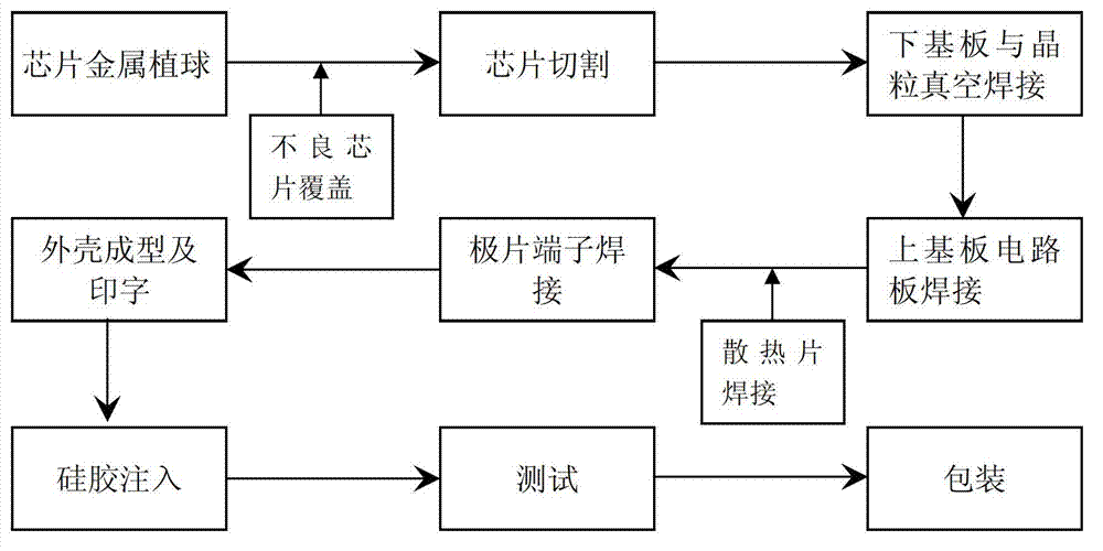
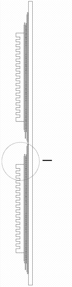
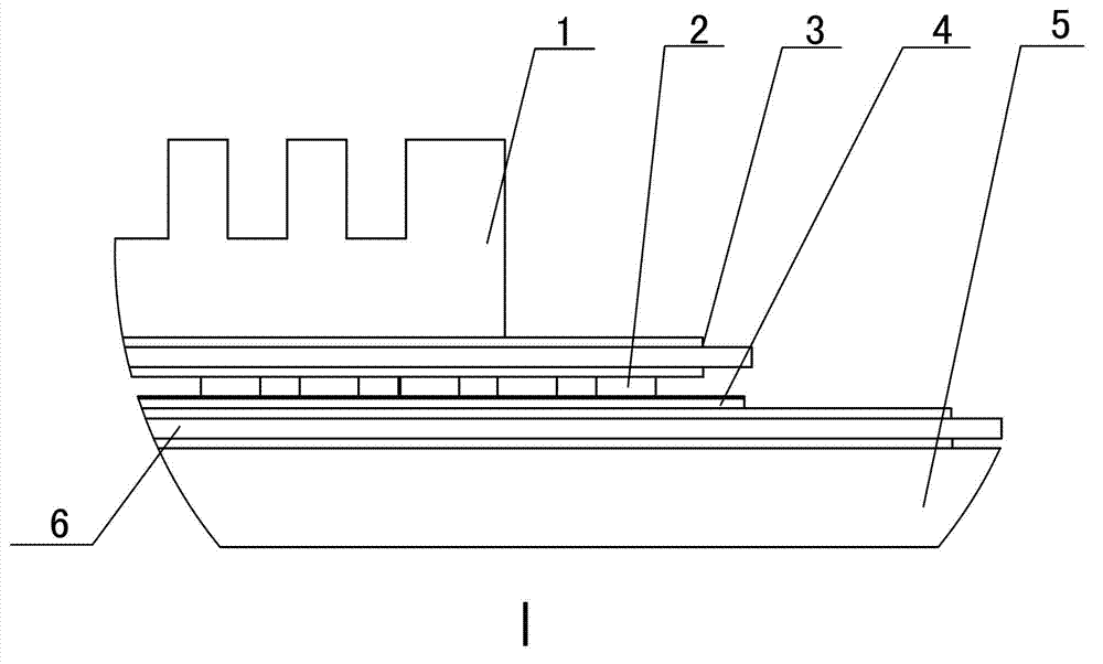
[0031] Figure 1-3 , 5-8 is the best embodiment of the IGBT module packaging process and the IGBT module of the present invention, below in conjunction with the attached Figure 1-8 The present invention will be further described.

[0032] Refer to attached Figure 1-8 :

[0033] The IGBT module of the present invention is composed of an upper heat sink 1, a metal ball 2, an upper substrate 3, a chip 4, a lower heat dissipation plate 5 and a lower substrate 6, and a metal ball 2 is implanted on the chip 4, and the metal ball 2 directly connects the chip 4 with the The upper substrate 3 with lines is connected, and a heat dissipation device is arranged above the metal ball 2 . The heat dissipation device includes an upper substrate 3 and an upper heat sink 1 above it. Both the upper substrate 3 and the lower substrate 6 are ceramic copper clad laminates. The upper heat sink 1 is fin-shaped.

[0034] Refer to attached Figure 4 and Figure 5 :

[0035] Figure 4 It is ...


PUM


Abstract

The invention discloses an IGBT (insulated gate bipolar translator) module packaging process and an IGBT module with bidirectional heat radiation, belonging to the technical field of semiconductor device manufacturing. The process comprises the following steps: step 1.1, implanting a metal ball (2) on a chip (4); step 1.2, covering bad chips and cutting the chip; step 1.3, welding a lower substrate (6) with crystalline grains in a vacuum mode; step 1.4, welding an upper substrate (3) with the chip; step 1.5 welding the upper substrate with an upper heat radiation fin (1); and step 1.6, welding pole piece terminals, molding a shell and printing words on the shell, injecting silica gel, testing and packaging. The process has the advantages that by adopting the chip metal implanted ball technique, the damage to the chip is reduced as no metal line is used, and with the adoption of the IGBT module manufactured by using the advanced process, the heat radiation of a product is increased by additionally arranging the heat radiation fin externally, and the module efficiency and the pass percent are increased, etc.

Description

technical field [0001] The invention discloses an IGBT module packaging process and a two-way heat dissipation IGBT module, belonging to the technical field of semiconductor device manufacturing, and specifically relates to a new NOW PAK IGBT (insulated gate bipolar transistor) module and packaging process. Background technique [0002] like Figure 9 As shown, the traditional insulated gate bipolar transistor IGBT module packaging adopts the method of punching metal wires 7 to connect the chips in parallel and in series to achieve the purpose of increasing the current and voltage of the module. This method is very easy to cause damage to the high-power IGBT chip (chip area If the soldering of the chip is slightly uneven, the chip will be damaged), and the upper part of the chip cannot be connected to the heat sink, and the heat dissipation effect is poor. It is easy to cause product failure due to temperature rise during use. Contents of the invention [0003] The techni...

Claims


Application Information

Patent Timeline
Patent Type & Authority Applications(China)
IPC IPC(8): H01L21/60H01L21/331H01L23/492H01L23/488H01L29/739
CPCH01L2924/1305H01L2924/13055H01L2224/48091H01L2224/49111H01L2924/00014H01L2924/00
Inventor 吕新立关仕汉
Owner 淄博美林电子有限公司
Why Eureka
Try Eureka