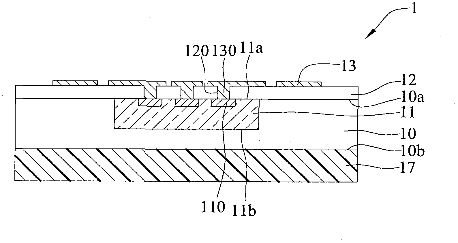
Chip-scale package
A technology of chip size packaging and packaging, which is applied in the direction of electrical components, electric solid devices, semiconductor devices, etc., and can solve the problem of poor distribution and diffusion of the build-up dielectric layer 12 and the inability of the build-up dielectric layer 12 to be evenly distributed and covered Layer 10, delamination and other problems to achieve the effect of avoiding delamination, good adhesion, and improving reliability
- Summary
- Abstract
- Description
- Claims
- Application Information
AI Technical Summary
Problems solved by technology
Method used
Image
Examples
no. 1 example
[0064] see figure 2 , which is a chip-scale package 2 of the present invention, which includes: a cladding layer 20 having opposite first surfaces 20a and second surfaces 20b, embedded in the first surface 20a of the cladding layer 20 and exposed At least one chip 21 on the first surface 20a of the cladding layer 20, a buffer dielectric layer (Buffer Dielectric Layer) 22 formed on the first surface 20a of the cladding layer 20 and the chip 21, and the The wiring layer 23 on the buffer dielectric layer 22 .
[0065] The material of the cladding layer 20 is encapsulation colloid or soft material, and in this embodiment, the soft material is Ajinomoto Build-up Film (ABF), Bismaleimide-Triacine (BT), polyimide ( Polyimide, PI), silicone resin (polymerized siloxanes, silicone) or epoxy resin.
[0066] The chip 21 has an opposite active surface 21a and a non-active surface 21b, and has a plurality of electrode pads 210 on the active surface 21a of the chip 21, and the chip 21 is ...
no. 2 example
[0077] see image 3 , the difference between this embodiment and the first embodiment lies in the related design of the newly added substrate 30 , and the structures and materials of other related packages are the same, so details are not repeated here.
[0078] The package 3 is combined with a substrate 30 on the second surface 20 b of the cladding layer 20 and the non-active surface 21 b of the chip 21 .
[0079] The substrate 30 has an upper surface 30a and a lower surface 30b, the upper and lower surfaces 30a, 30b are respectively provided with circuits 31, 32 electrically connected to each other, and the upper surface 30a is bonded to the first layer of the cladding layer 20. On the two surfaces 20b and the non-active surface 21b of the chip 21, the circuit 31 of the upper surface 30a is embedded in the cladding layer 20, and the circuit 31 of the upper surface 30a has a plurality of conductive components 33, with electrical properties The conductive blind hole 230 ′ of ...
no. 3 example
[0085] see Figure 4 and Figure 4 ', the difference between this embodiment and the first embodiment lies in the related design of the newly added conductive bumps 40, 40', and the structures and materials of other related packages are the same, so no more details are given here.
[0086] The packages 4, 4' form conductive bumps 40, 40' in the cladding layer 20, and the upper ends of the conductive bumps 40, 40' are combined with the buffer dielectric layer 22 and the lower ends are exposed to the cladding. The second surface 20b, 20b' of the layer 20, 20' is used to combine the conductive component (for example: metal wire, solder, solder ball) 46, and the circuit layer 23 is electrically connected to the conductive bump 40 through the conductive blind hole 230' , 40' upper end.
[0087] In this embodiment, the conductive bumps 40, 40' are made of copper.
[0088] In addition, a metal layer 41 can be formed on the lower surface of the conductive bump 40 to combine with th...
PUM
 Abstract
Description
Claims
Application Information
 - R&D
- Intellectual Property
- Life Sciences
- Materials
- Tech Scout
- Unparalleled Data Quality
- Higher Quality Content
- 60% Fewer Hallucinations
Browse by: Latest US Patents, China's latest patents, Technical Efficacy Thesaurus, Application Domain, Technology Topic, Popular Technical Reports.
© 2025 PatSnap. All rights reserved.Legal|Privacy policy|Modern Slavery Act Transparency Statement|Sitemap|About US| Contact US: help@patsnap.com


