Insulated gate bipolar transistor with dielectric layer at collector terminal

A technology of bipolar transistors and dielectric layers, applied in circuits, electrical components, semiconductor devices, etc., can solve problems such as device avalanche breakdown, device shutdown failure, device temperature rise, etc., to reduce hole injection, current Concentration suppression, area reduction effect

Inactive Publication Date: 2012-12-19
UNIV OF ELECTRONIC SCI & TECH OF CHINA +1
View PDF5 Cites 17 Cited by
  • Summary
  • Abstract
  • Description
  • Claims
  • Application Information

AI Technical Summary

Problems solved by technology

At this time, for the terminal region of the IGBT device, a large number of holes are injected into the drift region from the collector of the device. Concentration at the bit ring, thus forming a local accumulation effect of hole current at the equipotential ri

Method used


Image

  • Insulated gate bipolar transistor with dielectric layer at collector terminal
  • Insulated gate bipolar transistor with dielectric layer at collector terminal
  • Insulated gate bipolar transistor with dielectric layer at collector terminal

Examples


Embodiment Construction

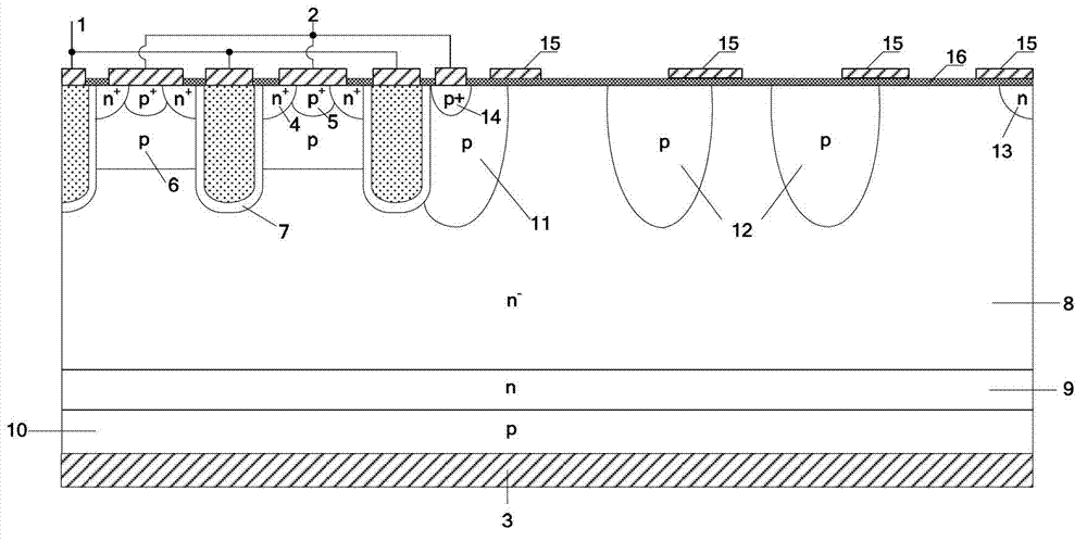
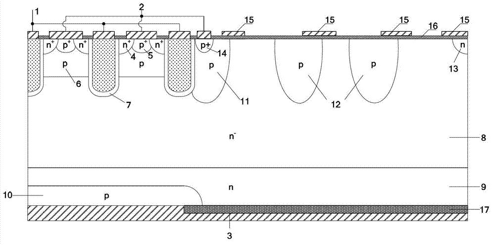
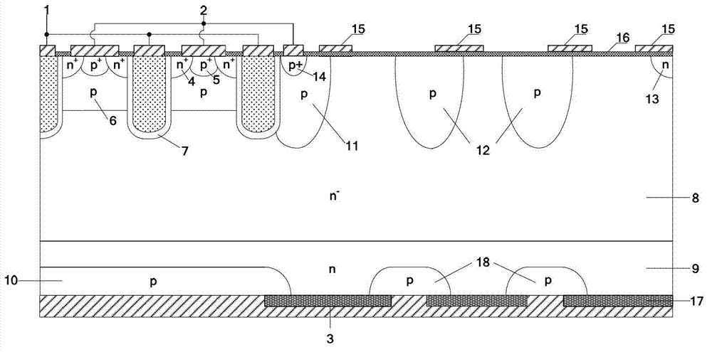
[0024] An insulated gate bipolar transistor with a dielectric layer at the collector terminal, such as Figure 2 to Figure 5 As shown, the collector termination region of the IGBT has a dielectric layer 17; the dielectric layer 17 is specifically located at the termination region of the P-type collector region 10 or the termination region of the metal collector 3.

[0025] In the above scheme:

[0026] The dielectric layer 17 can be a continuous structure or a discontinuous structure.

[0027] The dielectric layer 17 can be silicon oxide, silicon nitride, silicon oxynitride, borophosphosilicate glass and other dielectric materials.

[0028] The length, width, thickness and shape of the dielectric layer 17 can be changed accordingly according to design requirements.

[0029] The gate electrode of the insulated gate bipolar transistor may be a planar gate, a trench gate, or a planar gate or a trench gate with a carrier storage layer.

[0030] The collector of the IGBT may be ...


PUM


Abstract

The invention discloses an insulated gate bipolar transistor with a dielectric layer at a collector terminal, belonging to the technical field of power semiconductor devices and power integrated circuits. According to the invention, a continuous or discontinuous dielectric layer is introduced into a region of the terminal collector of a device on the basis of a traditional structure of the insulated gate bipolar transistor. According to the invention, the effective hole emission efficiency in the region of the terminal collector of the device can be significantly reduced due to the dielectric layer introduced, so that the hole injections at the terminal of the device can be reduced. When the device is cut off, the phenomenon of current concentration around an equipotential ring of the terminal of the device can be effectively inhibited due to the reduction of the hole injections in the region of the collector of the terminal, so that the thermal breakdown and the dynamic avalanche breakdown caused by the current concentration can be inhibited and eliminated, the cut-off ability of the insulated gate bipolar transistor can be effectively improved, and the reliability of the device can be improved.

Description

technical field [0001] The invention belongs to the technical field of power semiconductor devices and power integrated circuits, and relates to an insulated gate bipolar transistor (IGBT). Background technique [0002] Insulated gate bipolar transistors (IGBTs) are widely used in frequency conversion and speed control devices in fields such as communications, energy, transportation, industry, medicine, and household appliances. They are one of the core electronic components in modern power electronic circuits. As a new type of power electronic device combining MOS field effect and bipolar transistor, IGBT not only has the advantages of easy driving and simple control of MOSFET, but also has the advantages of reduced conduction voltage of power transistor, large on-state current and small loss. Since it came out in the 1980s, it has developed rapidly. The large-scale application of IGBT plays an extremely important role in improving the performance of power electronic syste...

Claims


Application Information

Patent Timeline
IPC IPC(8): H01L29/739H01L29/08
Inventor 张金平李巍夏小军安俊杰张灵霞李泽宏任敏张波
Owner UNIV OF ELECTRONIC SCI & TECH OF CHINA
Why Eureka
Try Eureka