
Grid voltage bootstrapped switch circuit

A gate voltage bootstrap and switching circuit technology, applied in the field of integrated circuits, can solve problems such as greater influence on circuit sampling accuracy, unfavorable capacitor C1 voltage, and limited charging speed, so as to reduce charging and discharging time, reduce signal distortion, reduce non-linear effect

Inactive Publication Date: 2012-12-19
INST OF SEMICONDUCTORS - CHINESE ACAD OF SCI
View PDF3 Cites 20 Cited by
  • Summary
  • Abstract
  • Description
  • Claims
  • Application Information

AI Technical Summary

Problems solved by technology

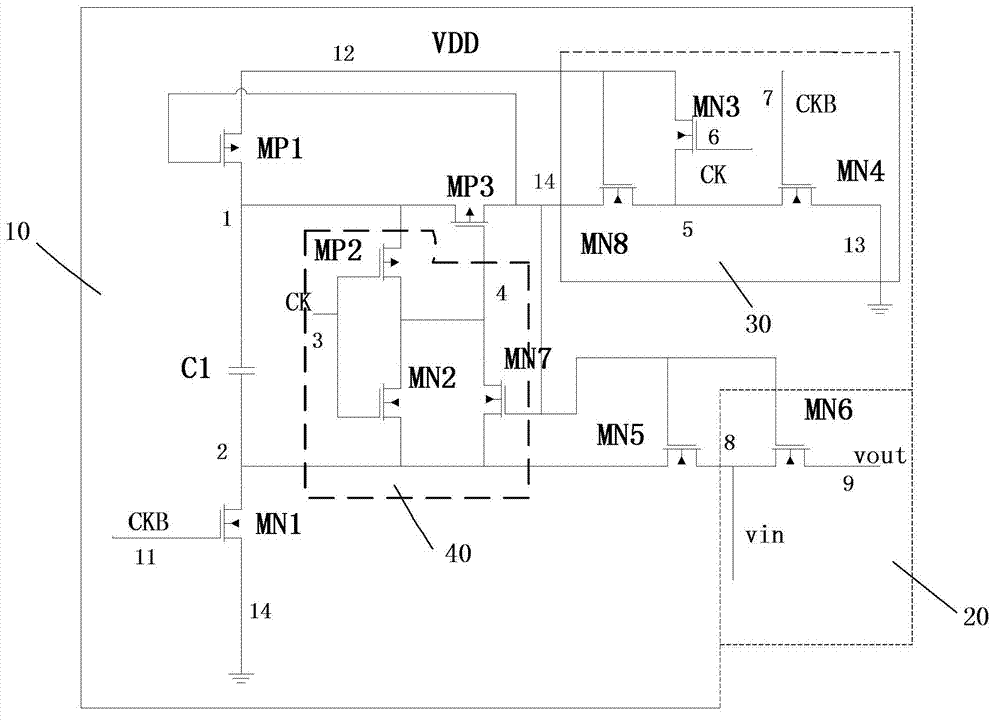
[0010] However, considering that when the CK signal becomes low and the CKB signal becomes high, the MP2 transistor is turned on, and the fourth node 4 is charged to a high level, and the charging charge comes from the stored charge of the capacitor C1, which is very unfavorable for the voltage of the capacitor C1 hold, which has a great influence on the sampling accuracy of the circuit
In addition, in the gate charge charging and discharging circuit 30 of the NMOS switch tube 20, the fast charging path includes MN8 and MN3, and the path resistance is relatively large, which seriously limits the charging speed.

Method used


Image

  • Grid voltage bootstrapped switch circuit
  • Grid voltage bootstrapped switch circuit
  • Grid voltage bootstrapped switch circuit

Examples


Embodiment Construction

[0034] In order to make the object, technical solution and advantages of the present invention clearer, the present invention will be described in further detail below in conjunction with specific embodiments and with reference to the accompanying drawings.

[0035] It should be noted that, in the drawings or descriptions of the specification, similar or identical parts all use the same figure numbers. Implementations not shown or described in the accompanying drawings are forms known to those of ordinary skill in the art. Additionally, while illustrations of parameters including particular values ​​may be provided herein, it should be understood that the parameters need not be exactly equal to the corresponding values, but rather may approximate the corresponding values ​​within acceptable error margins or design constraints.

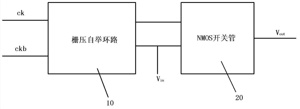
[0036] image 3 It is a schematic structural diagram of a gate voltage bootstrap switch circuit according to an embodiment of the present invention. ...


PUM


Abstract

The invention provides a grid voltage bootstrapped switch circuit. The grid voltage bootstrapped switch circuit comprises a grid voltage bootstrapped loop circuit (10) and an NMOS (N-Metal Oxide Semiconductor) switching tube (MN6), wherein the grid voltage bootstrapped loop circuit (10) is used for generating grid control voltage under the control of a clock signal, and the grid control voltage can be influenced by an input analog signal; and a grid end of the NMOS switching tube (MN6) is connected with the grid voltage bootstrapped circuit (10), a leakage end of the NMOS switching tube (MN6) is connected to an analog signal input end, a source end of the NMOS switching tube (MN6) is connected to a discrete signal output end, and the NMOS switching tube (MN6) is used for keeping the grid source voltage difference unchanged under the control of the grid control voltage, sampling the analog signal input by the analog signal input end into a discrete signal and outputting the discrete signal from the discrete signal output end. According to the grid voltage bootstrapped switch circuit provided by the invention, the nonlinearity of switching on a resistor by a switch is removed to the maximum, the signal distortion is reduced, and the circuit accuracy is increased.

Description

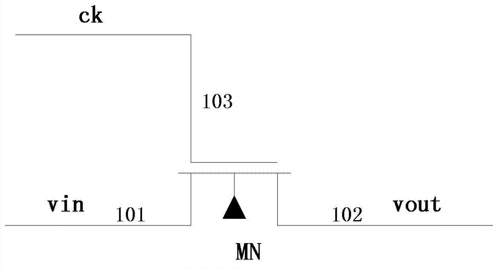
technical field [0001] The invention relates to the technical field of integrated circuits, in particular to a gate voltage bootstrap switch circuit realized by a CMOS process. Background technique [0002] With the development of technology, high-speed and high-precision has become the design goal of the analog-to-digital converter, and the sample-and-hold circuit is the core part of the analog-to-digital converter, and its performance determines the performance of the entire analog-to-digital converter. Therefore, it is particularly important to design a high-speed and high-precision sample-and-hold circuit. The most critical in the sample and hold circuit is undoubtedly the sampling switch. [0003] In CMOS technology, traditional sampling switches such as figure 1 As shown, it is an NMOS transistor MN, and the source 1 of the NMOS transistor is the analog signal input terminal V in , the drain 2 of the NMOS transistor is the discrete signal output terminal V out , an...

Claims


Application Information

Patent Timeline
Patent Type & Authority Applications(China)
IPC IPC(8): H03K17/687
Inventor 马波袁凌曹晓东张强郝志坤石寅
Owner INST OF SEMICONDUCTORS - CHINESE ACAD OF SCI
Learn More