
FPGA (Field Programmable Gate Array)-based Roberts edge detector
An edge detector and controller technology, applied in the direction of instruments, data conversion, electrical digital data processing, etc., can solve the problems of high implementation cost of edge detection software, large consumption of hardware resources, slow operation speed, etc., to achieve clear effect and realize Simple, smooth video effects
- Summary
- Abstract
- Description
- Claims
- Application Information
AI Technical Summary
Problems solved by technology
Method used
Image

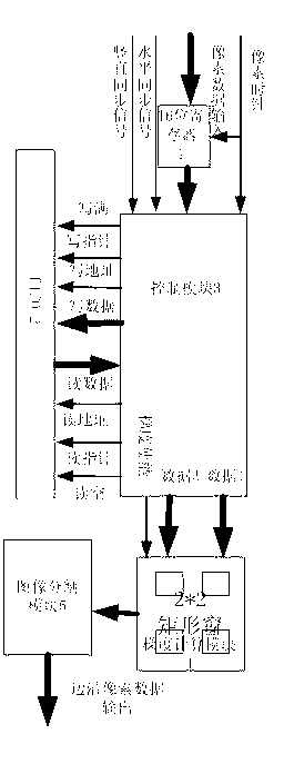


Examples
Embodiment 1
[0032] Such as figure 1 As shown, this FPGA-based Roberts edge detector consists of a 16-bit register (1), a function-specific synchronous FIFO (2), a core controller module (3), a gradient calculation module (4) and an image segmentation module (5). The core controller module (3) is connected to the synchronous FIFO (2), and the gradient calculation module (4) is connected to the image segmentation module (5). At the sending end, the input pixel data is cached by a 16-bit register and a synchronous FIFO (2) with a depth of "640", and then two rows of pixels are simultaneously input to the gradient calculation module (4), so that the difference between the two pixels is "640" pixels, Then two pixels enter the gradient calculation module (4) to realize When the square window is full, calculate the gradient value of the pixel at the point, and input the gradient value to the image segmentation module (5), compare it with the set threshold (T), realize edge extraction and imag...
Embodiment 2
[0034] This embodiment is basically the same as Embodiment 1, and the special features are as follows:
[0035] , synchronous FIFO (2)
[0036] see figure 2 , image 3 , Figure 4 , the entire FIFO structure diagram is as follows figure 2 , including FIFO storage unit (2-3), write address controller (2-2), read address controller (2-4) and FIFO state controller (2-1), FIFO state controller (2-1) Connect the FIFO write address controller (2-2), FIFO storage unit (2-3) and read address controller (2-4), triggered by the rising edge of the pixel clock, to achieve simultaneous read and write operations. Write Address Controller (2-2) as image 3 , a frequency divider by two, a comparator, an adder, a latch, two binary selectors and an AND gate. Read address controller as Figure 4 , a frequency divider by two, a comparator, an adder, a latch, two binary selectors and an AND gate.
[0037] The write address is generated by the write address controller (2-2), the init...
PUM
 Abstract
Description
Claims
Application Information