Low-power-consumption xor/xnor gate circuit

A gate circuit, low-power technology, applied in the field of low-power XOR/XOR gate circuits, can solve the problems of increasing the number of transistors and circuit power consumption, and achieve the effect of reducing the number of transistors and reducing power consumption

Inactive Publication Date: 2013-01-02
NINGBO UNIV
View PDF3 Cites 19 Cited by
  • Summary
  • Abstract
  • Description
  • Claims
  • Application Information

AI Technical Summary

Problems solved by technology

like figure 2 As shown, the XOR gate circuit is composed of four inverters and two transmission gates. All the PMOS transistors and NMOS transistors in this circuit are transistors with the minimum channel length under the 130nm standard process, but because the XOR gate The circuit uses multiple inverters, resulting in an increase in the number of transistors in the circuit, which leads to an increase in power consumption of the circuit

Method used


Image

  • Low-power-consumption xor/xnor gate circuit
  • Low-power-consumption xor/xnor gate circuit
  • Low-power-consumption xor/xnor gate circuit

Examples


Embodiment 1

[0024] Embodiment 1: As shown in the figure, a low-power XOR / XOR gate circuit includes an input inverter module 1, a complementary transmission tube logic module 2 and a differential series voltage switch logic module 3, and the input inverter module 1 includes the first PMOS transistor P1, the first NMOS transistor N1, the second PMOS transistor P2 and the second NMOS transistor N2, and the complementary transmission transistor logic module 2 includes the third NMOS transistor N3, the fourth NMOS transistor N4, and the fifth NMOS transistor N5 and the sixth NMOS transistor N6, the differential series voltage switching logic module 3 includes a third PMOS transistor P3 and a fourth PMOS transistor P4, the source of the first PMOS transistor P1, the source of the second PMOS transistor P2, the third PMOS transistor P3 The source of the fourth PMOS transistor P4 and the source of the power supply positive terminal V DD connected, the source of the first NMOS transistor N1 and th...

Embodiment 2

[0025]Embodiment 2: other parts are the same as Embodiment 1, the difference is: under the SMIC130nm standard process, the channel length of the first PMOS transistor P1, the channel length of the second PMOS transistor P2, and the channel length of the third PMOS transistor P3 The channel length, the channel length of the fourth PMOS transistor P4, the channel length of the first NMOS transistor N1, the channel length of the second NMOS transistor N2, the channel length of the third NMOS transistor N3, the channel length of the fourth NMOS transistor N4 The channel length, the channel length of the fifth NMOS transistor N5 and the channel length of the sixth NMOS transistor N6 are all 135nm.

Embodiment 3

[0026] Embodiment 3: other parts are the same as Embodiment 1, the difference is that: under the SMIC130nm standard process, the channel length of the first PMOS transistor P1, the channel length of the second PMOS transistor P2, and the channel length of the third PMOS transistor P3 The channel length, the channel length of the fourth PMOS transistor P4, the channel length of the first NMOS transistor N1, the channel length of the second NMOS transistor N2, the channel length of the third NMOS transistor N3, the channel length of the fourth NMOS transistor N4 The channel length, the channel length of the fifth NMOS transistor N5 and the channel length of the sixth NMOS transistor N6 are all 139nm.

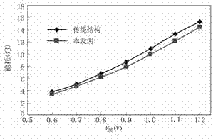
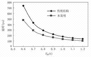
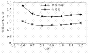
[0027] In order to compare the performance characteristics of the XOR / NOR gate circuit of the present invention with respect to the standard unit XOR gate circuit released by the SMIC130nm process, under the standard process of SMIC130nm, the circuit simulation tool HSPICE was used...


PUM


Abstract

The invention discloses a low-power-consumption xor/xnor gate circuit which is characterized by comprising an input inverter module, a complementary transmission tube logic module and a differential series voltage switch logic module. The input inverter module is connected with the complementary transmission tube logic module which is further connected with the differential series voltage switch logic module. The low-power-consumption xor/xnor gate circuit has the advantages that transistors of the circuit are reduced without affecting circuit performances, so that power consumption of the circuit is effectively reduced. Further, the low-power-consumption xor/xnor gate circuit not only has xor logic functions but also has xnor logic functions.

Description

technical field [0001] The invention relates to an exclusive OR / exclusive OR gate circuit, in particular to a low power consumption exclusive OR / exclusive OR gate circuit. Background technique [0002] The power consumption of CMOS circuits has become one of the biggest challenges in the field of integrated circuit design. In recent years, with the rapid development of chip technology, the feature size of the chip has entered the nanoscale. The continuous improvement of circuit operating speed and scale, as well as the exponential growth of leakage power consumption, lead to a sharp increase in chip power consumption. Reducing chip power consumption has become a key technical problem that needs to be solved urgently. A sharp increase in the chip's power consumption can cause many problems. The temperature rise caused by the increase of power consumption of the chip will reduce the reliability of the components on the chip, thereby reducing the stability of the chip, and wi...

Claims


Application Information

Patent Timeline
Patent Type & Authority Applications(China)
IPC IPC(8): H03K19/20H01L29/06
Inventor 胡建平陈金丹杨丹
Owner NINGBO UNIV
Why Eureka
Try Eureka