

Fast recovery diode and manufacturing method thereof
A technology for recovering diodes and semiconductors, applied in semiconductor/solid-state device manufacturing, electrical components, circuits, etc., to achieve the effects of reducing the conductance voltage drop, enhancing the conductance modulation effect, and slowing down the rising trend
- Summary
- Abstract
- Description
- Claims
- Application Information
AI Technical Summary
Problems solved by technology
Method used
Image

Examples
Embodiment
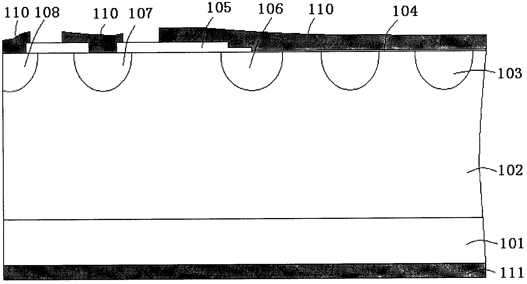
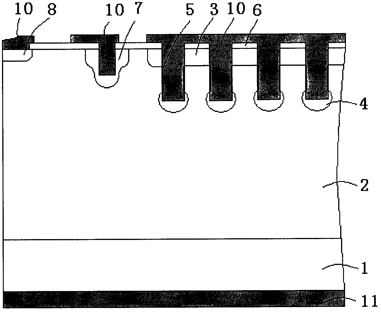
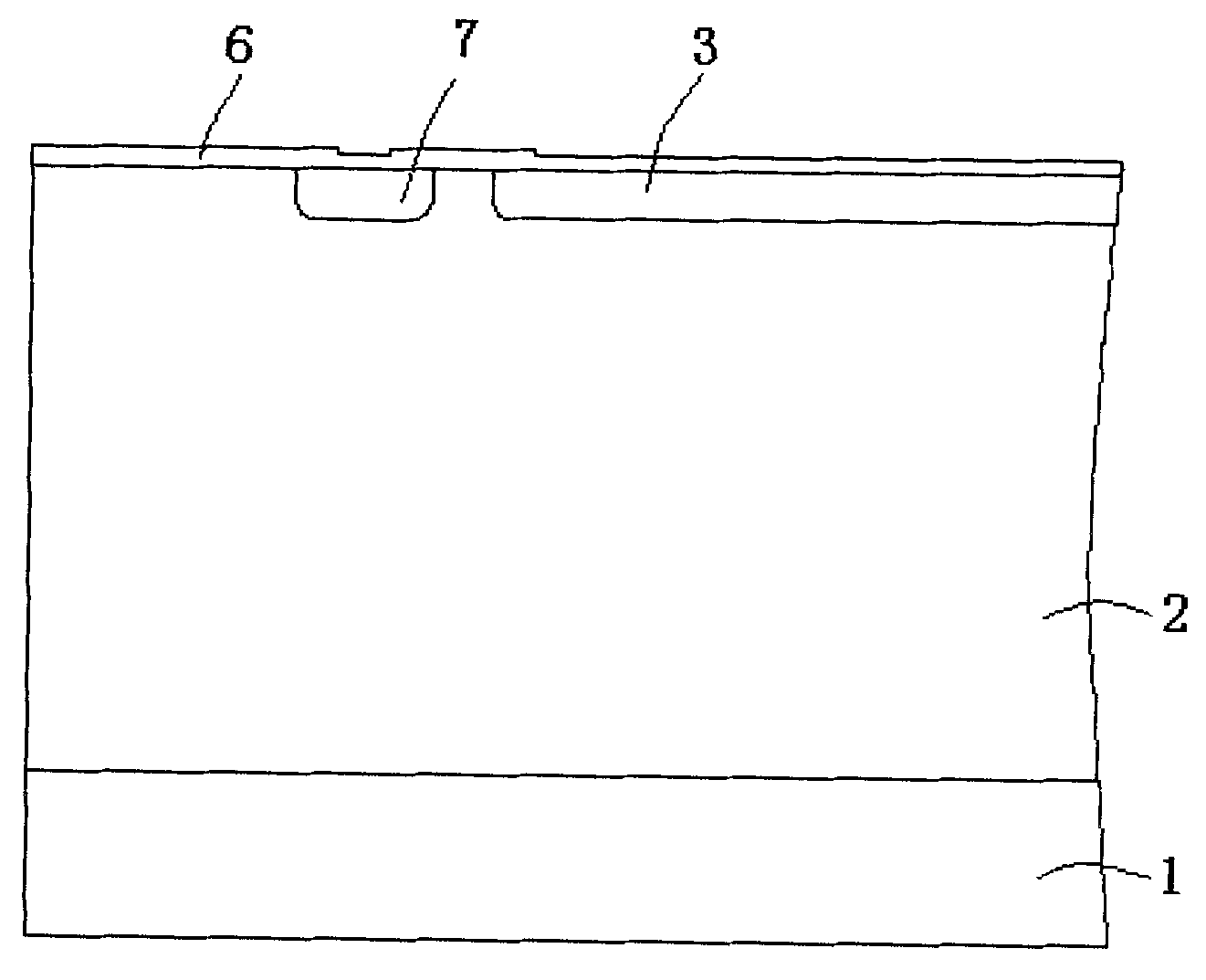
[0034] figure 2 It is a schematic cross-sectional view of a fast recovery diode of the present invention, which includes: an N-type conductive semiconductor silicon material substrate layer 1, which is a heavily doped N-conductive type silicon semiconductor material, and the phosphorus doping concentration is 1E19cm -3 ; The upper surface of the N-type conductive semiconductor silicon material substrate layer 1 is an N-type conductive semiconductor silicon material drift layer 2, and the phosphorus doping concentration is 2E14cm -3 , with a thickness of 60 μm; the first P-type region 3, located in the upper part between the trenches, is a P-type conductive semiconductor silicon material, with a junction depth of 1.5 μm; the second P-type region 4, located at the bottom of the trench, is P-type conductive Semiconductor silicon material, junction depth of 1μm; Schottky barrier junction 5, located on the sidewall of the trench, trench depth of 4μm, width of 2μm, Schottky barrier...
PUM
 Abstract
Description
Claims
Application Information