

Method for co-plating metallization of blind holes and through hole of printed circuit board
A printed circuit board and metal plating technology, which is applied in the direction of the electrical connection of printed components, can solve the problems of excessive copper filling sag in blind holes and small hole diameters, and achieve the elimination of blind hole copper filling sags, increase productivity and Production efficiency and production cost reduction effect
- Summary
- Abstract
- Description
- Claims
- Application Information
AI Technical Summary
Problems solved by technology
Method used
Image

Examples
Embodiment approach 1
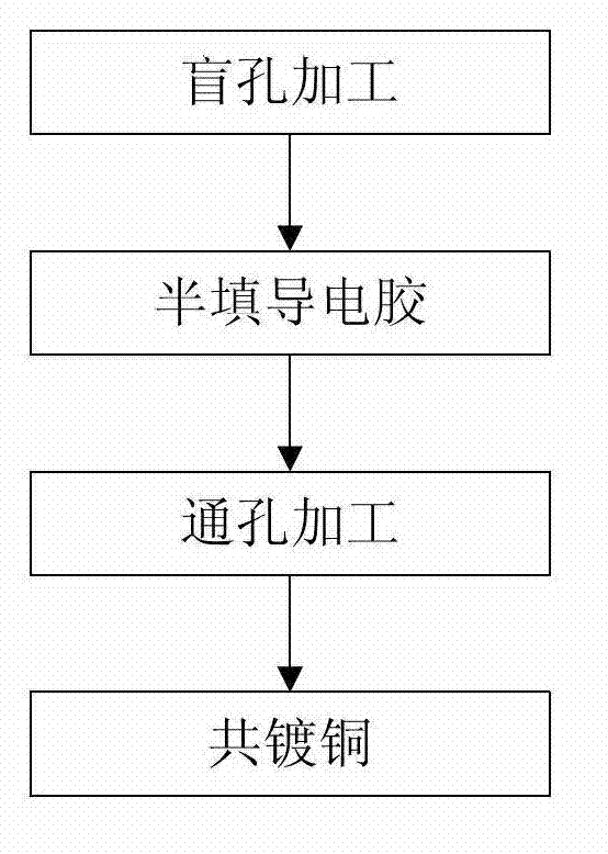
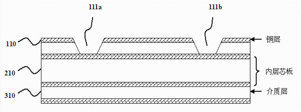
[0042] Such as Figure 2-6 As shown, the through hole and blind hole co-plating metallization method in the present embodiment 1 comprises the following steps:
[0043] Step 1. Laminate the copper foil layer 110, the inner core layer 210, and the dielectric layer 310. After the lamination, a printed circuit board with copper layers on both sides is formed, and laser drill blind holes on the printed board. 111, the dielectric material 310 used can be FR-4 material or PTFE material;
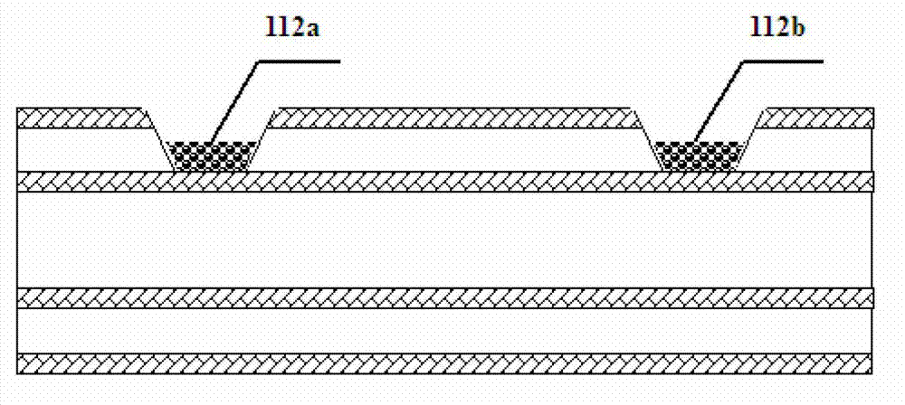
[0044]Step 2. Half-fill the conductive adhesive 112 in the blind hole drilled above the laser hole. Before printing the conductive adhesive with the printing machine, adjust the height of the scraper to realize the controlled depth of the conductive adhesive, so that the blind hole can be half-filled. The conductive adhesive can be epoxy resin conductive adhesive with stable conductivity and high bonding strength, and the conductive adhesive can be cured;
[0045] Step 3. Carry out mechanical dri...
Embodiment approach 2
[0051] Such as Figure 2-6 As shown, the co-plating metallization method for through holes and blind holes in Embodiment 2 includes the following steps:
[0052] Step 1. Laminate the copper foil layer 110, the inner core layer 210, and the dielectric layer 310. After lamination, a printed circuit board with copper layers on both sides is formed, and laser drill blind holes on the printed board. 111, the dielectric material 310 used can be FR-4 material or PTFE material;
[0053] Step 2. Half-fill the conductive adhesive 112 in the blind hole drilled above the laser hole. Before printing the conductive adhesive with the printing machine, adjust the height of the scraper to realize the controlled depth of the conductive adhesive, so that the blind hole can be half-filled. The conductive adhesive can be epoxy resin conductive adhesive with stable conductivity and high bonding strength, and the conductive adhesive can be cured;
[0054] Step 3. Carry out mechanical drilling thro...
PUM
 Abstract
Description
Claims
Application Information