Electromagnetic wave absorber, method of producing the same, flexible printed wiring board and electronic device

A manufacturing method and absorber technology, applied in the direction of printed circuit, printed circuit, printed circuit dielectric, etc., can solve the problems of increased electromagnetic noise, electronic equipment failure, cancer, etc., and achieve the effect of high electromagnetic wave absorption

Inactive Publication Date: 2013-01-16
SONY CORP
View PDF4 Cites 6 Cited by
  • Summary
  • Abstract
  • Description
  • Claims
  • Application Information

AI Technical Summary

Problems solved by technology

[0002] In recent years, with the miniaturization and high operating speed of electronic equipment, electromagnetic noise generated from various electromagnetic waves emitted from electronic equipment has disadvantageously increased
In addition, it has been reported that electromagnetic noise can not only cause malfunctions of electronic equipment, but also cause leukemia, cancer, etc.

Method used


Image

  • Electromagnetic wave absorber, method of producing the same, flexible printed wiring board and electronic device
  • Electromagnetic wave absorber, method of producing the same, flexible printed wiring board and electronic device
  • Electromagnetic wave absorber, method of producing the same, flexible printed wiring board and electronic device

Examples


Embodiment 2

[0023] 3. Example 2 (flexible printed wiring board according to an embodiment of the present invention and electronic device according to an embodiment of the present invention) and others

[0024] [The electromagnetic wave absorber according to the first or second embodiment of the present invention, the flexible printed wiring board according to the embodiment of the present invention, the electronic device according to the embodiment of the present invention, the electromagnetic wave absorber according to the first or second embodiment of the present invention Absorbent manufacturing method, overview]

[0025] In the electromagnetic wave absorber according to the first or second embodiment of the present invention, the electromagnetic wave absorber of the flexible printed wiring board according to the embodiment of the present invention and the electromagnetic wave absorber of the electronic device according to the embodiment of the present invention desirably contain 100 pa...

Embodiment 1

[0087] Example 1 of the present invention relates to the electromagnetic wave absorber according to the first or second embodiment of the present invention, and the manufacturing method of the electromagnetic wave absorber according to the first or second embodiment of the present invention.

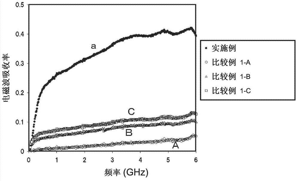
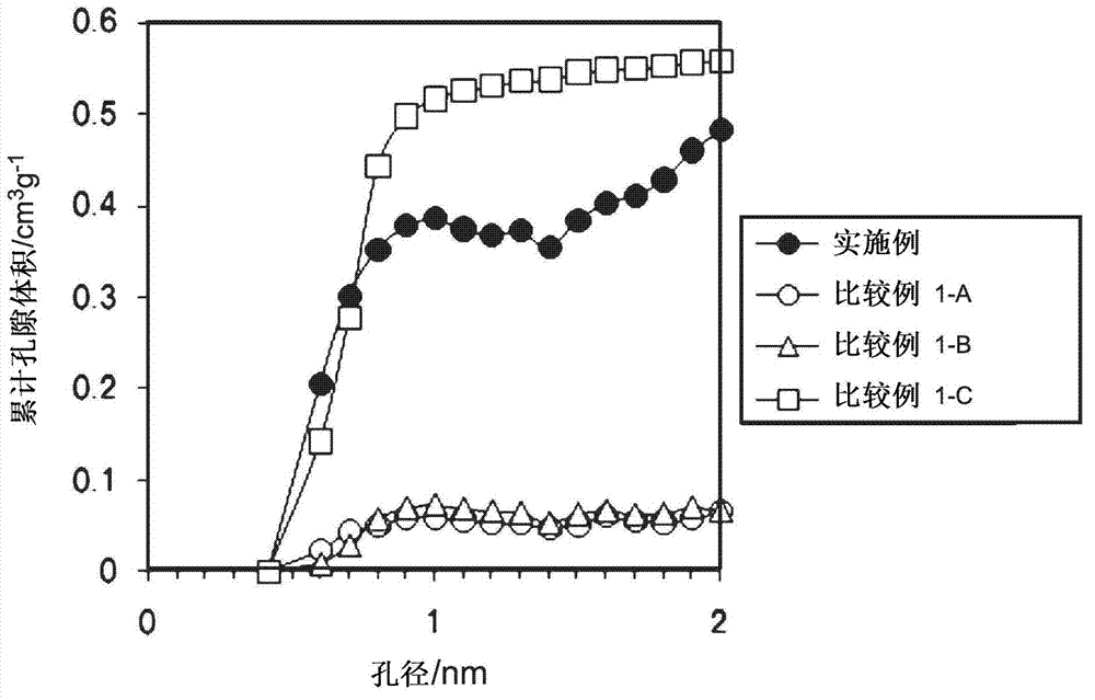
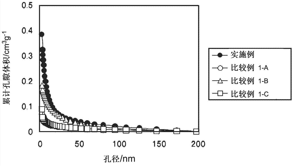
[0088] As expressed according to the first embodiment of the present invention, Example 1 of the present invention is an electromagnetic wave absorber comprising a base material and a porous carbon material comprising a plant-based The material is used as a raw material, wherein the specific surface area value of the porous carbon material measured by the nitrogen BET method is 400m 2 / g or more, a silicon (Si) content of 1% or more by mass, and a pore volume measured by the BJH method of 0.2 cm 3 / g or more, and the pore volume measured by the MP method is 0.2cm 3 / g or more.

[0089]As expressed according to the second embodiment of the present invention, Example 1 of the present inv...


PUM

PropertyMeasurementUnit
specific surface areaaaaaaaaaaa
pore sizeaaaaaaaaaa
specific surface areaaaaaaaaaaa

Abstract

Provided is an electromagnetic wave absorber, including a base material and a porous carbon material containing, as a raw material, a plant-based material having a silicon content of 5% by mass or more, in which the porous carbon material has a specific surface area value as measured by the nitrogen BET method of 400 m2/g or more, a silicon content of 1% by mass or less, a pore volume as measured by the BJH method of 0.2 cm3/g or more, and a pore volume as measured by the MP method of 0.2 cm3/g or more, or a total pore volume of pores each having a diameter in the range from 110-9 m to 510-7 m as measured by the Non Localized Density Functional Theory of 1.0 cm3/g or more.

Description

technical field [0001] The present invention relates to an electromagnetic wave absorber, a manufacturing method thereof, a flexible printed wiring board, and electronic equipment. Background technique [0002] In recent years, with miniaturization and high operating speed of electronic equipment, electromagnetic noise generated by various electromagnetic waves emitted from electronic equipment has disadvantageously increased. In addition, it has been reported that electromagnetic noise can not only cause malfunction of electronic equipment, but also cause leukemia, cancer, etc. As a means for solving these problems of electromagnetic noise, for example, an electromagnetic wave absorber can be applied to electronic equipment. The mechanism by which an electromagnetic wave absorber absorbs electromagnetic waves utilizes conductivity, dielectricity, or magnetism. Various electromagnetic wave absorbers have been developed. [0003] Among them, attention is paid to electromag...

Claims


Application Information

Patent Timeline
Patent Type & Authority Applications(China)
IPC IPC(8): H05K9/00H05K1/02C01B31/02
CPCH05K1/02C01B31/02H05K1/0218H05K9/0083H05K2201/0116C01B31/00H05K2201/0715H05K9/00H05K2201/0323H01Q17/002C01B32/00
Inventor 饭田广范山之井俊凑屋街子田畑诚一郎山田心一郎管野正喜三木理和加藤义宽
Owner SONY CORP
Why Eureka
Try Eureka