Manufacturing method of semiconductor component

A component manufacturing and semiconductor technology, which is applied in the field of semiconductor component manufacturing, can solve problems such as difficult removal of the surface of the substrate and gate structure, etc.

Inactive Publication Date: 2013-01-23
UNITED MICROELECTRONICS CORP
View PDF0 Cites 3 Cited by
  • Summary
  • Abstract
  • Description
  • Claims
  • Application Information

AI Technical Summary

Problems solved by technology

However, since it is often difficult to remove the residues on the surface of the substrate and the gate structure during the subsequent cleaning process of the photoresist material, how to improve such deficiencies is the main purpose of the present invention

Method used


Image

  • Manufacturing method of semiconductor component
  • Manufacturing method of semiconductor component
  • Manufacturing method of semiconductor component

Examples


Embodiment Construction

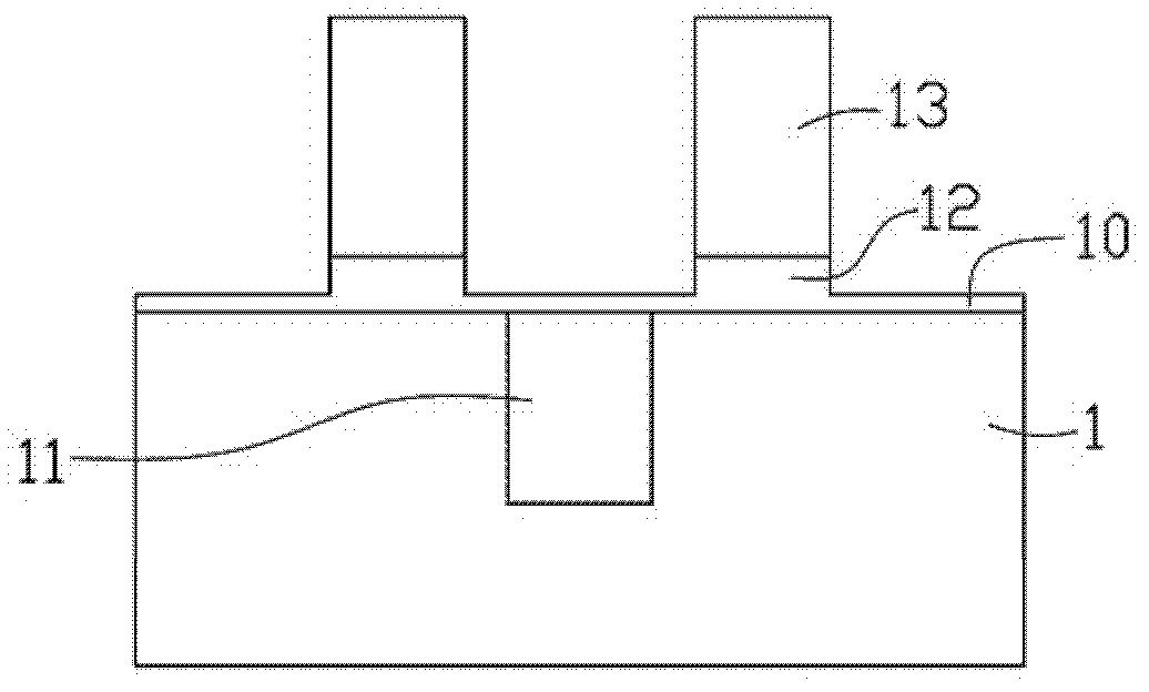
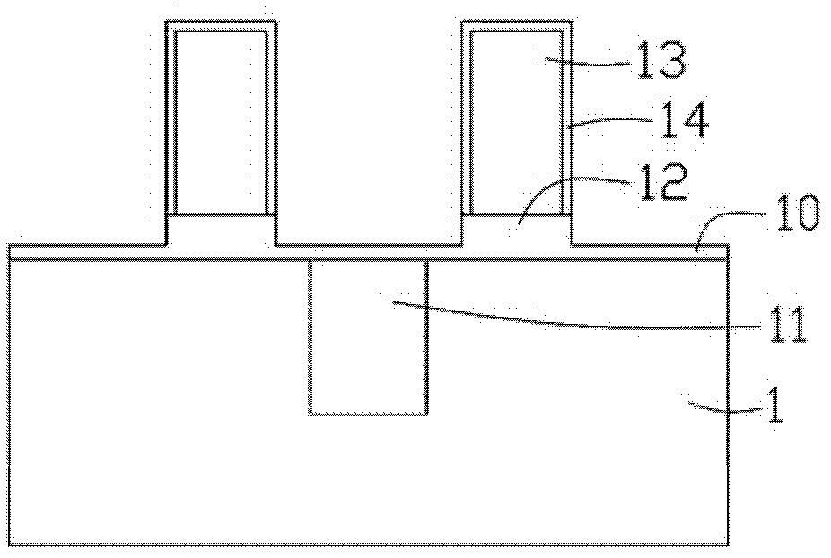
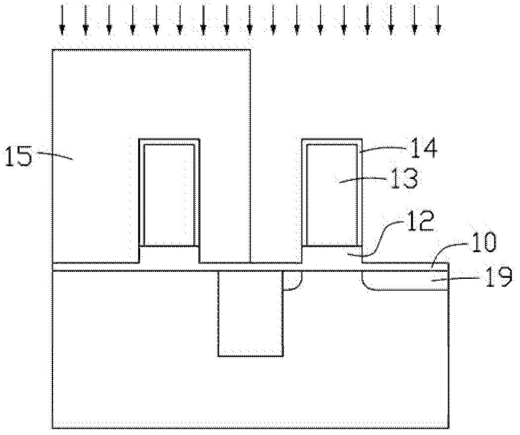
[0026] See Figure 1A ~ Figure 1F , which is a schematic flow diagram of part of the process of manufacturing a semiconductor element. first, Figure 1A It shows that after the shallow trench isolation structure 11 is completed on the silicon substrate 1 , the gate dielectric layer 12 and the silicon gate structure 13 are fabricated on the surface of the silicon substrate 1 . The silicon oxide layer 10 is silicon oxide remaining after the definition of the silicon gate structure 13 and the gate dielectric layer 12 is completed. In addition, the silicon gate structure 13 is a structure containing silicon, which may include uniform or gradient or heterogeneous Polycrystalline silicon, monocrystalline silicon, doped silicon, epitaxy of silicon and other elements or doped materials such as silicon germanium material, strained silicon, or any combination of the above. Also, although the silicon gate structure 13 shown in the figure is a single-layer structure, it can be a multi-la...


PUM

PropertyMeasurementUnit
thicknessaaaaaaaaaa
thicknessaaaaaaaaaa

Abstract

The invention discloses a manufacturing method of a semiconductor component. The manufacturing method comprises the steps of providing a substrate, wherein a silicon gate structure is formed on the substrate; conducting a modification technology on a silicon surface of the silicon gate structure, so that the characteristic of the silicon surface of the silicon gate structure is changed to hydrophily from hydrophobicity; forming a mask structure on the substrate; conducting a dopant injecting technology on the substrate by the silicon gate structure after the modification technology and the mask structure; and removing the mask structure by a mask structure removal technology, wherein the mask structure removal technology comprises a wet clean step. According to the manufacturing method of the semiconductor component, as the surface characteristic of the silicon gate structure is changed into the hydrophily, the residue after an ashing treatment can be removed and cleaned smoothly by the wet clean step.

Description

technical field [0001] The invention relates to a method for manufacturing a semiconductor element, in particular to a method for manufacturing a semiconductor element used in an integrated circuit process. Background technique [0002] In integrated circuits, metal-oxide-semiconductor transistors are commonly used circuit components, and in the manufacturing process, the gate structure is usually used as a mask for ion implantation. In the CMOS transistor process, it is often necessary to use a photoresist material to cover a specific area, so as to achieve the purpose of implanting different dopants in different areas of the substrate. However, since it is often difficult to remove the residues on the surface of the substrate and the gate structure during the subsequent cleaning process of the photoresist material, how to improve such deficiencies is the main purpose of the present invention . Contents of the invention [0003] In order to improve the above disadvantag...

Claims


Application Information

Patent Timeline
Patent Type & Authority Applications(China)
IPC IPC(8): H01L21/336
Inventor 刘安淇
Owner UNITED MICROELECTRONICS CORP
Why Eureka
Try Eureka