Surface mounting welding process for wafer-level chip

A surface mount and soldering process technology, which is applied in the direction of assembling printed circuits, electrical components, and electrical solid devices with electrical components, can solve the problems of low process cost reliability and high material, and achieve the goal of avoiding cost and process time Effect

Inactive Publication Date: 2013-02-06
XIAMEN RXD ELECTRONICS
View PDF2 Cites 12 Cited by
  • Summary
  • Abstract
  • Description
  • Claims
  • Application Information

AI Technical Summary

Problems solved by technology

[0005] Aiming at the problems of high material and process costs and low reliability caused by the above-mentioned packaging process, the main purpose of the present invention is to provide a manufacturing method for surface mount soldering of bare crystals to solve the problem of large-scale application of bare crystals in production. Because of the above problems caused by packaging, the technical solution is as follows:

Method used


Image

  • Surface mounting welding process for wafer-level chip
  • Surface mounting welding process for wafer-level chip
  • Surface mounting welding process for wafer-level chip

Examples


Embodiment 1

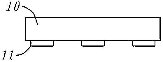
[0041] figure 1 , figure 2 As shown, in the bare crystal 10 used in the first embodiment, a metal electrode 11 for soldering is provided on the bottom surface of the bare crystal 10 .

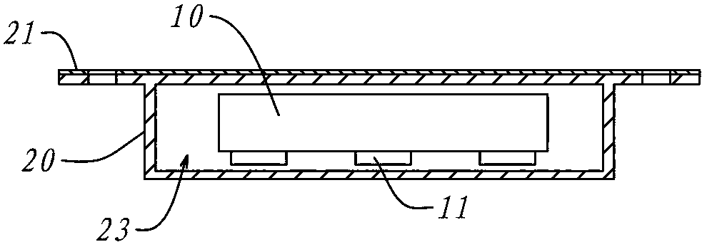
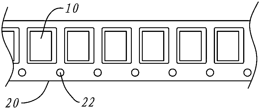
[0042] Such as figure 2 and image 3 As shown, in the step of arranging, the bare crystals 10 are placed one by one into the temporary storage container 20 for storage. The temporary storage container 20 used in this embodiment has a linear braiding structure, and the elongated braiding is provided with multiple The accommodating spaces 23 are arranged in a straight line, each bare die 10 occupies one accommodating space 23 , and are independent from each other; and the metal electrodes 11 of the bare dies 10 all face the bottom of the accommodating spaces 23 . When the bare crystal 10 is placed into the accommodating space 23 , there will be a protective film 21 at the opening of the temporary storage container 20 to seal the accommodating space 23 for protection. The braiding has a posi...

Embodiment 2

[0056] Such as Figure 9 to Figure 12 , is a partial process diagram of Embodiment 2 of the present invention.

[0057] From Figure 9 It can be seen that the metal electrode of the die 10 has a portion extending on the side of the die 10, and, Figure 10 and Figure 11 It is shown that the temporary storage container 20 used by the bare die 10 is in the form of a tray, so the bare die 10 is distributed in the accommodation space 23 of the temporary storage container 10 in an array, and its metal electrodes 11 are also oriented toward the container. bottom of the space.

[0058] The placement steps of this embodiment are the same as those of Embodiment 1, and Figure 12 shows that the solder paste 50 is not only interposed between the metal electrode 11 and the pad 31, but also has a part attached to the metal electrode 11 on the side of the bare crystal 10. This welding method has high mechanical strength and a large solder joint current. In particular, from Figure 12 ...


PUM


Abstract

The invention discloses a surface mounting welding process for a wafer-level chip, which is characterized by comprising the following steps of: firstly, providing the wafer-level chip with a flip chip structure and placing the wafer-level chip into a temporary storage container, wherein one surface of the chip is provided with a metal electrode and the metal electrode also can comprise a part extending to the lateral surface of the chip; then providing a substrate, wherein the substrate is provided with a matchable pad and solder paste is arranged on the pad in advance in a steel mesh printing manner; sucking the chip from the temporary storage container by adopting a vacuum suction nozzle and placing the chip on the pad of the substrate; temporarily fixing the metal electrode of the chip on the substrate by utilizing the surface tension of the solder paste; and finally, communicating the pad and the metal electrode which are temporarily fixed together in a reflow soldering manner. According to the technical scheme, the post packaging process step and the cost of the wafer-level chip are saved, the competitiveness of a product is promoted, existing SMT (Surface Mounting Technology) equipment can be basically continuously used, additional hardware do not need to be greatly invested, the cost of a packaging line and the process time are avoided, and the mass production of the wafer-level chip is easy to implement.

Description

technical field [0001] The invention relates to a process for direct surface mount welding of bare crystal (wafer level chip). Background technique [0002] With the development of semiconductor technology, large-scale / ultra-large-scale integrated circuits are widely used in many fields, which directly leads to the development of chip packaging technology, which is characterized in that wafer-level chips that have been etched and grown ( Bare crystal) is packaged in a special shell, so that when the chip is applied to a specific circuit substrate, it can be directly connected to the electrodes on the package, such as tin welding, butt welding, etc. This method has formed a mature process, which can enable small-volume bare crystals to be directly used by downstream manufacturers through a common soldering process. [0003] Therefore, the packaging process of bare die has become an indispensable step in the production process of modern integrated circuits. On the one hand, i...

Claims


Application Information

Patent Timeline
Patent Type & Authority Applications(China)
IPC IPC(8): H01L21/60H05K3/34
CPCH01L24/81H01L24/11H01L24/13H01L24/16H01L24/75H01L2224/11005H01L2224/1132H01L2224/13294H01L2224/133H01L2224/16225H01L2224/16227H01L2224/75745H01L2224/81048H01L2224/81192H01L2224/81815H01L2224/81907
Inventor 廖泳黄锦良
Owner XIAMEN RXD ELECTRONICS
Why Eureka
Try Eureka